
ADI 5962-8770002EA
- Quad 8-bit voltage-output DAC with on-chip output buffer amplifiers — four channels on one die
- Laser-trimmed amplifier offsets — no external offset nulling or user trimming required
- Common 8-bit TTL/CMOS compatible data bus with individual latches for each DAC channel
- Single or dual supply operation with reference voltage range of 2V to 12.5V
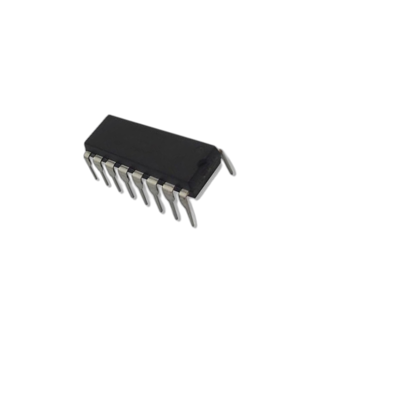
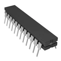
- MIL-STD-883 Class B qualified under SMD 5962-87802 — 20-lead ceramic SOIC package
- Military temperature range: –55°C to +125°C
Four independent DAC channels, one die, no external trimming — that is the core proposition of the ADI 5962-8770002EA. It is the military SMD procurement designation for Analog Devices' AD7226TE processed to MIL-STD-883 Class B, housed in a 20-lead ceramic SOIC package and rated for the full military temperature range. Built on Analog Devices' LC2MOS process — the same high-speed linear-compatible CMOS technology used in the AD7572S — it integrates precision analog DAC circuitry and high-speed digital control logic on a single monolithic chip without the performance compromises that typically come with mixed-signal integration.
What makes the AD7226 architecture practical for military system designs is the combination of channel density and interface simplicity. All four DACs share a common 8-bit TTL/CMOS data bus, with address lines A0 and A1 selecting which channel is loaded when WR goes low — a control scheme that is directly compatible with most 8-bit military microprocessors without glue logic. Each channel's output amplifier is laser-trimmed at manufacture, eliminating the offset nulling circuits and calibration procedures that discrete DAC implementations require. With reference voltage flexibility from 2V to 12.5V and support for both unipolar and bipolar output configurations, the 5962-8770002EA adapts to a wide range of military analog output requirements from a single qualified component.
Related Products For Your Business
Four precision DAC channels in a single military-qualified package — the ADI 5962-8770002EA solves a problem that comes up repeatedly in military analog output design: how to drive multiple independent analog signals from one component without sacrificing precision, microprocessor compatibility, or qualification traceability. Processed to MIL-STD-883 Class B under SMD 5962-87802, it provides a standardized DoD acquisition path for programs that need qualified quad DAC capability across the military temperature range.
5962-8770002EA Architecture: LC2MOS Quad DAC With Laser-Trimmed Outputs
The AD7226 LC2MOS process that underlies the 5962-8770002EA was designed specifically to integrate high-speed digital logic and precision analog circuitry on the same substrate — a combination that typically requires careful process tradeoffs. The four output buffer amplifiers are laser-trimmed during manufacture to achieve their specified offset performance, which means there is nothing to calibrate at board assembly and nothing that drifts out of specification as the system ages. The shared 8-bit data bus with individual per-channel latches allows any of the four outputs to be updated independently or simultaneously, and the latch architecture holds each output stable at its last programmed value while other channels are being updated — a behaviour that matters in military systems where analog output glitching during digital writes can cause downstream control problems.
5962-8770002EA Interface and Configuration Flexibility
The microprocessor interface of the 5962-8770002EA is direct and undemanding: a TTL/CMOS compatible 8-bit data bus, two address lines, and an active-low write strobe — the same signals available on virtually every 8-bit military processor and DSP bus without additional logic. Reference voltage flexibility from 2V to 12.5V covers most analog output range requirements, and the device supports both unipolar and bipolar output configurations through simple external resistor networks. For designs that also require precision voltage referencing, the 5962-9078501MLA AD780S precision reference and the 5962-9451801MLA AD7572S 12-bit ADC complement the 5962-8770002EA in a complete military mixed-signal signal chain.
Sourcing the ADI 5962-8770002EA
The 5962-8770002EA is a legacy military DAC with sustained demand in long-lifecycle defense and avionics programs where qualified analog output components are difficult to substitute without redesign. We maintain verified inventory with full lot traceability, MIL-STD-883 certificate of conformance, and anti-counterfeit inspection on every order. Whether the requirement is a small prototype quantity or a production lot, our team responds within 24 hours with pricing and availability. Contact us today to request a quote for the ADI 5962-8770002EA.
- Quad channel architecture reduces component count versus discrete single-channel DAC implementations
- Laser-trimmed output amplifiers — no offset nulling, no calibration, no external trim components
- Individual per-channel latches hold outputs stable during writes to other channels
- Direct microprocessor bus interface — TTL/CMOS compatible, no glue logic required
- Unipolar and bipolar output configurations supported through external resistor networks
- MIL-STD-883 Class B qualification with full lot traceability documentation
- 20-lead ceramic SOIC package — hermetic construction for military environmental reliability
- Complements 5962-9078501MLA and 5962-9451801MLA in complete military mixed-signal designs
Frequently Asked Questions (FAQ)
What Is the ADI 5962-8770002EA and What Is Its Commercial Equivalent?
The 5962-8770002EA is the military SMD procurement designation for Analog Devices’ AD7226TE, processed to MIL-STD-883 Class B under drawing 5962-87802. It is a quad 8-bit voltage-output DAC with laser-trimmed output amplifiers, a common microprocessor-compatible data bus, and individual per-channel latches, rated for military operation from –55°C to +125°C in a 20-lead ceramic SOIC package.
How Does the Quad DAC Architecture of the 5962-8770002EA Work?
All four DAC channels share a single 8-bit data bus. When a write occurs, address lines A0 and A1 determine which of the four channels receives the new data. Each channel has its own latch, so its output holds at the last programmed value until explicitly updated — there is no interaction between channels during write operations, and no output glitching on channels that are not being addressed.
Does the 5962-8770002EA Require External Trimming or Calibration?
No. The output buffer amplifiers are laser-trimmed at manufacture to achieve their specified offset performance. No external offset nulling components or user calibration procedures are required to meet the datasheet specifications — the device performs to specification straight from qualified stock.
What Is the Difference Between the 5962-8770002EA and the Commercial AD7226TE?
The electrical specifications are identical. The 5962-8770002EA designation indicates MIL-STD-883 Class B processing and screening, with full qualification documentation including lot traceability and certificate of conformance. Commercial AD7226TE parts can be ordered to 883B screening by adding /883B to the part number, but the 5962 SMD number is the standardized acquisition path for DoD programs procuring from the qualified sources list.
How Do I Request a Quote for the ADI 5962-8770002EA?
Submit an inquiry through our website contact form or email our sales team directly. We will respond within 24 hours with pricing, availability, and lead time — and can discuss long-term supply agreements for production programs.