
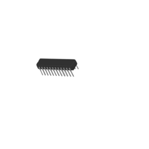
ADI 5962-8866302LA
- Pin-programmable precision voltage reference with four selectable outputs: 2.5V, 5V, 7.5V, and 10V
- Laser wafer trimmed output levels and temperature coefficients — no external adjustment required
- Unique strobe terminal enables output switching with a single low-power logic signal
- Wide input voltage range: 4.5V to 30V with 1 mA to 10 mA output current capability
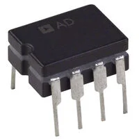
- MIL-STD-883 Class B qualified under SMD 5962-88663 — 8-lead hermetic TO-99 metal can
- Military temperature range: –55°C to +125°C
Most precision voltage reference designs lock the engineer into a single output voltage at the time of component selection. The ADI 5962-8866302LA takes a different approach. As the military SMD procurement designation for Analog Devices' AD584S processed to MIL-STD-883 Class B, it offers pin-programmable selection of four standard output voltages — 2.5V, 5V, 7.5V, and 10V — from a single 8-terminal TO-99 metal can package. Output voltage selection is made by connecting or leaving open specific programming pins, with no external resistors required for the four standard voltages. This flexibility means one qualified component can serve multiple reference requirements across a military system design, simplifying the bill of materials and reducing the number of distinct qualified parts that must be managed and stocked.
The AD584 architecture centers on a precision 1.215V bandgap reference driving a laser-trimmed op-amp feedback network. Laser wafer trimming of both initial accuracy and temperature coefficient is performed at the wafer level, resulting in tight specifications across the full –55°C to +125°C military range without user calibration. The strobe terminal — a feature unique to the AD584 — allows the output to be switched to zero with a single low-power signal, enabling power supply sequencing, reference switching, and system power management functions that would otherwise require additional discrete components.
Related Products For Your Business
A single qualified component that covers four standard reference voltages — that is the practical value proposition of the ADI 5962-8866302LA in military system design. For programs managing a qualified parts list, fewer distinct reference part numbers means fewer qualification records, fewer procurement relationships, and fewer obsolescence risks to track. The AD584S architecture achieves this without compromise: laser wafer trimming delivers tight temperature coefficient performance across the military range, and the four standard output voltages are set by pin connections alone, with no external resistors degrading accuracy or adding board area.
5962-8866302LA Architecture: Bandgap Reference With Laser-Trimmed Output Network
The AD584 builds its output voltage flexibility on a stable 1.215V bandgap core. A precision laser-trimmed resistor network around an on-chip op-amp multiplies this reference to each of the four programmable output levels — the same trimming approach that Analog Devices uses across its military precision reference portfolio. Because the trim is performed at the wafer level before packaging, the device arrives in its hermetic TO-99 can already calibrated to specification, with no post-assembly adjustment required or possible. For the 2.5V output, the 5962-8866302LA can also operate in a 2-terminal Zener configuration — connecting input and output to run as a shunt reference, which expands its applicability to negative reference and current source configurations that the 3-terminal mode cannot serve.
5962-8866302LA in Military Mixed-Signal Signal Chains
The AD584 has a long history as the external reference source for military ADC and DAC designs that require higher accuracy than their on-chip references can provide. For designs using the 5962-9451801MLA AD7572S 12-bit ADC — which includes an on-chip buried Zener reference — the 5962-8866302LA provides an alternative high-accuracy external reference path where the system accuracy budget demands it. Similarly, in designs using the 5962-8770002EA AD7226 quad DAC or the 5962-8778902EA AD7524 multiplying DAC, the 5962-8866302LA’s pin-selectable 2.5V or 5V output serves as a stable, qualified reference source that brings the full signal chain under a single MIL-STD-883 qualification framework.
Sourcing the ADI 5962-8866302LA
The AD584 in its military TO-99 hermetic package has been in continuous use in defense programs for decades, and the 5962-8866302LA remains an active procurement item for both legacy board repairs and new designs that benefit from its established qualification history. We maintain verified inventory with full lot traceability, MIL-STD-883 certificate of conformance, and anti-counterfeit inspection. Contact us today to confirm availability and request a quote for the ADI 5962-8866302LA — our team responds within 24 hours.
- Four standard output voltages from one package — simplifies qualified parts list management
- Strobe terminal enables output switching without additional discrete switching components
- 2-terminal Zener mode available at 5V output and above for negative reference applications
- Laser wafer trimmed at wafer level — no post-assembly calibration possible or required
- Output current up to 10 mA — sufficient to drive most ADC and DAC reference inputs directly
- 8-lead hermetic TO-99 metal can — proven military packaging for harsh environment reliability
- Compatible reference source for AD7572S, AD7226, and AD7524 military signal chain designs
- Full lot traceability and MIL-STD-883 certificate of conformance on every order
Frequently Asked Questions (FAQ)
What Is the ADI 5962-8866302LA and What Is Its Commercial Equivalent?
The 5962-8866302LA is the military SMD procurement designation for Analog Devices’ AD584S, processed to MIL-STD-883 Class B under drawing 5962-88663. It is a pin-programmable precision voltage reference offering selectable 2.5V, 5V, 7.5V, and 10V outputs in an 8-lead hermetic TO-99 metal can, rated for military operation from –55°C to +125°C. The commercial equivalents are the AD584S and AD584T.
How Does Pin Programming Work on the 5962-8866302LA?
The four standard output voltages are selected by connecting or leaving open specific programming pins on the 8-terminal package. No external resistors are required for the four standard outputs — the selection is made entirely through pin connections. Other output voltages above or between the standard values can be set by adding external resistors, as documented in the AD584 datasheet.
What Is the Strobe Terminal and How Is It Used in Military Designs?
The strobe terminal allows the reference output to be driven to zero by a single low-power logic signal — typically an NPN transistor driven by a TTL gate. In the off state, the device draws only approximately 100 µA, versus 750 µA in normal operation. This enables power supply sequencing, reference switching between system modes, and low-power standby states without external switching components.
How Does the 5962-8866302LA Compare to the 5962-9078501MLA AD780S?
Both are military-qualified precision voltage references, but they serve different design requirements. The 5962-9078501MLA AD780S provides a fixed 2.5V output with a tighter 3 ppm/°C maximum drift specification, making it the better choice when a single 2.5V reference with the lowest possible drift is the priority. The 5962-8866302LA AD584S offers pin-selectable outputs from 2.5V to 10V with a 15 ppm/°C maximum drift, making it the better choice when output voltage flexibility or the strobe function is needed across multiple reference requirements in a single design.
How Do I Request a Quote for the ADI 5962-8866302LA?
Submit an inquiry through our website contact form or email our sales team directly. We will respond within 24 hours with pricing, availability, and lead time — and can discuss long-term supply agreements for production programs.