
ADI 5962-8876401LA
- Ultra-low noise precision op amp — 3 nV/√Hz at 10 Hz, 80 nV p-p (0.1 Hz to 10 Hz)
- Exceptional input offset voltage: 25 µV maximum with 0.6 µV/°C maximum drift
- High gain-bandwidth product: 8 MHz with 2.8 V/µs slew rate
- Very high open-loop gain: 1.8 million V/V — outstanding closed-loop accuracy
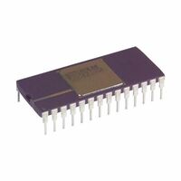
- MIL-STD-883 Class B qualified under SMD 5962-88764 — 8-lead hermetic TO-99 metal can
- Military temperature range: –55°C to +125°C
The ADI 5962-8876401LA is the military SMD procurement designation for Analog Devices' OP27E processed to MIL-STD-883 Class B, housed in an 8-lead hermetic TO-99 metal can and rated across the full military temperature range. The OP27 occupies a specific and important position in precision op amp history: it was the first device to combine the ultralow offset and drift performance of the OP07 with genuinely low noise — a combination that had previously required separate device selections with the attendant tradeoffs in gain, bandwidth, and board area. Decades later, the OP27 remains the reference point against which other precision low-noise amplifiers are benchmarked, and the 5962-8876401LA brings that performance into the DoD qualified parts framework under SMD 5962-88764.
The OP27E grade — the "E" suffix — specifies 25 µV maximum input offset voltage and 0.6 µV/°C maximum drift, the tightest available grade in the OP27 family. These specifications are guaranteed under MIL-STD-883 screening across the full –55°C to +125°C military temperature range, not just at 25°C. The combination of a 3 nV/√Hz broadband noise floor, a low 1/f corner frequency of 2.7 Hz, and an 8 MHz gain-bandwidth product makes the 5962-8876401LA a single-component solution for high-gain, low-noise precision amplification in military signal chains — from inertial sensor interfaces to radar front-end signal conditioning.
Related Products For Your Business
The OP27 set the standard for what a precision low-noise op amp should look like — low offset, low drift, low noise, and enough bandwidth to be useful in real signal chains. The ADI 5962-8876401LA delivers the E grade of that standard under MIL-STD-883 Class B: 25 µV maximum offset, 0.6 µV/°C maximum drift, and 3 nV/√Hz broadband noise, all guaranteed across the military temperature range in a hermetic TO-99 package. For programs that need a qualified single-channel precision op amp with a decades-long track record in defense electronics, the 5962-8876401LA is the established choice.
5962-8876401LA vs 5962-8872101PA: Single vs Dual Channel Selection
A common design decision in military signal chain layout is whether to use the OP27 (single channel) or the OP270 (dual channel) for a given amplification stage. The two devices share the same fundamental architecture and noise performance — the OP270 was specifically designed as the dual version of the OP27. The practical selection criteria are straightforward:
| 5962-8876401LA (OP27E) | 5962-8872101PA (OP270Z) | |
|---|---|---|
| Channels | 1 | 2 |
| Noise Density | 3 nV/√Hz @ 10 Hz | 5 nV/√Hz @ 1 kHz |
| Offset Voltage (max) | 25 µV | 75 µV |
| Offset Drift (max) | 0.6 µV/°C | 1 µV/°C |
| GBW | 8 MHz | 5 MHz |
| Package | TO-99 (L) | Ceramic DIP (P) |
| Best For | Single-channel, tightest offset/noise | Two-channel, power-conscious designs |
The OP27E in the 5962-8876401LA offers tighter offset and lower noise than the OP270Z — the single-channel architecture allows more aggressive trimming. For two-channel designs where the slight specification advantage of the OP27E matters, two 5962-8876401LA devices can be used; where board space or power consumption is the constraint, the 5962-8872101PA dual package is the more efficient choice.
5962-8876401LA in Military Precision Signal Chains
The OP27 has a long history as the input stage amplifier in military precision signal chains — placed ahead of ADCs to condition weak sensor signals before digitization, or used as the output amplifier for DAC stages where low offset and accurate gain are required. In designs using the 5962-9451801MLA AD7572S 12-bit ADC, the 5962-8876401LA provides a low-noise, high-accuracy front-end amplification stage that preserves the ADC’s dynamic range. For reference-driven analog output stages using the 5962-8866302LA AD584S pin-programmable voltage reference, the OP27’s 1.8 million V/V open-loop gain supports the precise buffering and level-shifting that precision reference applications require.
Sourcing the ADI 5962-8876401LA
The OP27 in its military TO-99 hermetic package remains one of the most consistently specified legacy op amps in defense electronics, appearing in designs across every military platform category. We maintain verified inventory with full lot traceability, MIL-STD-883 certificate of conformance, and anti-counterfeit inspection. Contact us today to confirm availability and request a quote for the ADI 5962-8876401LA — our team responds within 24 hours.
- E grade specifies 25 µV maximum offset and 0.6 µV/°C maximum drift — tightest available OP27 grade
- 1/f corner frequency of 2.7 Hz — noise performance extends into the sub-10 Hz range critical for DC-coupled sensor interfaces
- Bias current cancellation circuit holds IB and IOS stable across the military temperature range
- Unity-gain stable — no external compensation required for any closed-loop configuration
- Output drives ±10V into 600Ω — sufficient for most military analog bus and interface requirements
- 8-lead TO-99 hermetic metal can — proven military packaging with excellent environmental isolation
- MIL-STD-883 Class B qualification with full lot traceability documentation
- Direct upgrade path from OP07 for designs requiring lower noise with comparable offset performance
Frequently Asked Questions (FAQ)
What Is the ADI 5962-8876401LA and What Is Its Commercial Equivalent?
The 5962-8876401LA is the military SMD procurement designation for Analog Devices’ OP27EZ, processed to MIL-STD-883 Class B under drawing 5962-88764. It is a single-channel ultra-low noise precision op amp with 3 nV/√Hz broadband noise density, 25 µV maximum input offset voltage, and 0.6 µV/°C maximum drift, rated for military operation from –55°C to +125°C in an 8-lead hermetic TO-99 metal can.
What Is the Difference Between the OP27 Grades (A, E, F, G)?
The OP27 family is offered in multiple accuracy grades that differ primarily in guaranteed input offset voltage and drift. The E grade specified by the 5962-8876401LA is the tightest: 25 µV maximum offset and 0.6 µV/°C maximum drift. The G grade relaxes these to 100 µV and 1.8 µV/°C respectively. For military precision applications where offset and drift directly affect system accuracy, the E grade provides the tightest performance guarantee.
How Does the 5962-8876401LA Compare to the OP07 in Military Designs?
The OP07 offers lower offset voltage (75 µV vs. 25 µV for the E grade) and comparable drift, but significantly higher noise — approximately 10 nV/√Hz versus 3 nV/√Hz for the OP27. The OP27 was specifically designed to improve on the OP07’s noise performance while retaining its precision, making the 5962-8876401LA the preferred choice when both low noise and low offset are required simultaneously.
Is the 5962-8876401LA Unity-Gain Stable?
Yes. The OP27 is unity-gain stable, requiring no external frequency compensation components in any closed-loop configuration. This simplifies circuit design and reduces external component count compared to decompensated amplifiers that require minimum gain constraints.
How Do I Request a Quote for the ADI 5962-8876401LA?
Submit an inquiry through our website contact form or email our sales team directly. We will respond within 24 hours with pricing, availability, and lead time — and can discuss long-term supply agreements for production programs.