ADI AD7892SQ-1
- 12-bit, 500 kSPS LC2MOS SAR ADC with on-chip T/H, internal 2.5V reference, and ±1 LSB INL
- ±10V and ±5V true bipolar input ranges with ±17V overvoltage protection on analog inputs
- Selectable parallel or serial interface — single pin switches between 12-bit bus and DSP serial mode
- Single +5V supply operation with 60 mW typical power dissipation
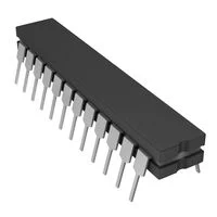
- 24-lead hermetic CDIP package rated –55°C to +125°C military temperature range
The ADI AD7892SQ-1 is the military temperature range CDIP variant of Analog Devices' AD7892 — a high-speed, low-power 12-bit LC2MOS SAR ADC with on-chip track-and-hold amplifier, internal 2.5V reference, and a dual-mode interface that switches between parallel and serial operation. The SQ suffix identifies the 24-lead hermetic ceramic DIP package with the extended –55°C to +125°C temperature rating, making it the correct procurement path for defense, avionics, and high-reliability programs that require the AD7892-1 architecture beyond the –40°C to +85°C industrial range. The -1 model specifier selects the ±10V and ±5V bipolar input ranges with ±17V overvoltage protection — the input range combination suited to military analog signal levels and defense sensor interfaces where transient overstress is a realistic operating condition.
The AD7892's dual-mode interface is the feature that most distinguishes it from single-mode alternatives in military system integration. The same package pin set supports both a standard parallel 12-bit bus interface with fast access times for microprocessor data bus connections and a high-speed serial interface for direct connection to DSP and microcontroller serial ports — mode selection is software and hardware configurable. Serial output format provides sixteen bits of data with four leading zeros preceding the 12 bits of valid conversion data, compatible with TMS320 and ADSP serial port framing protocols. Both DC accuracy specifications (INL, DNL, offset, gain) and AC dynamic performance (THD, SNR) are specified for the AD7892SQ-1, reflecting the LC2MOS architecture's ability to deliver both precision static accuracy and clean dynamic performance from a single +5V supply.
Related Products For Your Business
For defense procurement teams sourcing the AD7892SQ-1, the SQ suffix is the specification that matters most: hermetic CDIP packaging and –55°C to +125°C temperature rating in the same AD7892 architecture available in industrial plastic packages. The AD7892BN-1 and AD7892BR-1 industrial variants carry the same ±1 LSB INL specification and dual-mode interface, but are limited to –40°C to +85°C in plastic packaging — adequate for most industrial applications but insufficient for airborne, shipboard, or missile system environments where the military temperature range and hermetic sealing are non-negotiable requirements. The AD7892SQ-1 closes that gap without moving to a different ADC architecture or revalidating the signal conditioning design.
AD7892SQ-1 Architecture: Dual-Mode Interface and Bipolar Input on Single +5V Supply
The LC2MOS process that underlies the AD7892 combines precision bipolar analog circuitry with low-power CMOS logic — the combination that delivers both low-noise analog performance and the single +5V supply operation that simplifies power distribution in military embedded systems. The on-chip track-and-hold amplifier captures the analog input at the start of each 1.47 µs conversion cycle, handling input frequencies well beyond the Nyquist limit for the 500 kSPS conversion rate. The internal 2.5V reference is available at the REF IN/REF OUT pin for external use or external override — for designs where the internal reference drift is insufficient, a precision external reference such as the 5962-9078501MLA AD780S provides 3 ppm/°C maximum drift within the same military qualification framework. The dual-mode interface shares physical pins between parallel and serial functions, with the MODE pin determining which function is active — no external logic is required to configure the interface for either processor bus or DSP serial port connection.
AD7892SQ-1 vs AD7892 Family: Temperature and Package Selection
| AD7892SQ-1 | AD7892BN-1 | AD7892BR-1 | |
|---|---|---|---|
| Package | 24-Lead CDIP | 24-Lead PDIP | 28-Lead SOIC |
| Temperature | –55°C to +125°C | –40°C to +85°C | –40°C to +85°C |
| INL | ±1 LSB Maximum | ±1 LSB Maximum | ±1 LSB Maximum |
| Hermetic | Yes | No | No |
| Best For | Military / extended temp | Industrial cost-sensitive | Industrial SMT |
The AD7892SQ-1 is the correct choice when the military temperature range and hermetic ceramic packaging are both required. For industrial designs within –40°C to +85°C where plastic packaging is acceptable, the AD7892BN-1 or AD7892BR-1 provide the same electrical performance at lower cost. For single-channel precision acquisition at higher resolution, the AD7690BRMZ 18-bit PulSAR ADC and the AD7891ASZ-1 8-channel data acquisition system are complementary solutions for different acquisition architectures.
Sourcing the ADI AD7892SQ-1
The AD7892SQ-1 in its hermetic CDIP package maintains consistent demand in military avionics and defense programs where the –55°C to +125°C temperature range and ceramic packaging are specified requirements. We carry verified inventory with full lot traceability and anti-counterfeit inspection on every order. Contact us today to confirm availability and request a quote — our team responds within 24 hours.
- Hermetic CDIP package rated –55°C to +125°C — the only AD7892-1 variant for military temperature applications
- ±17V overvoltage protection survives sensor cable faults and transient events without device damage
- Dual-mode interface shares pins — no external logic required to switch between parallel and serial modes
- Serial output provides 16 bits with 4 leading zeros — compatible with TMS320 and ADSP serial port framing
- On-chip T/H handles input frequencies up to the Nyquist limit without external sample-and-hold
- Internal 2.5V reference available at REF IN pin for external signal chain use or external override
- Two’s complement output coding simplifies digital signal processing in bipolar input applications
- Full lot traceability and anti-counterfeit inspection on every order
Frequently Asked Questions (FAQ)
What Is the ADI AD7892SQ-1 and How Does It Differ From the AD7892BN-1?
The AD7892SQ-1 is the military temperature range variant of the AD7892-1 — a 12-bit, 500 kSPS LC2MOS SAR ADC with ±10V/±5V bipolar inputs, dual parallel/serial interface, and ±1 LSB INL in a 24-lead hermetic CDIP package rated for –55°C to +125°C. The AD7892BN-1 uses a plastic DIP package and is rated for –40°C to +85°C industrial operation. Both share identical electrical specifications — the difference is package and temperature range.
What Does the “-1” Suffix Mean on the AD7892SQ-1?
The -1 suffix specifies the ±10V and ±5V bipolar input range model. The AD7892-2 accepts 0V to +2.5V unipolar inputs; the AD7892-3 accepts ±2.5V bipolar inputs at a higher 600 kSPS throughput rate. All three models are available in the SQ hermetic CDIP package. Input range selection does not require hardware changes — it is fixed by the device model selected at procurement time.
How Does the Dual-Mode Interface Work on the AD7892SQ-1?
The MODE pin selects the interface type. In parallel mode, the 12-bit conversion result is available on DB11–DB0 with standard RD and CS control signals, with bus access times under 40 ns for direct microprocessor bus connection. In serial mode, the same physical pins become SCLK, RFS, TFS, and SDATA — providing a high-speed synchronous serial interface compatible with DSP and microcontroller serial ports. Mode switching requires only the MODE pin state change and corresponding firmware configuration.
Does the AD7892SQ-1 Require an External Reference?
No. The internal 2.5V reference drives the ADC core and is available at the REF IN/REF OUT pin. For applications requiring lower temperature drift, an external reference can override the internal reference via the REF IN pin. The 5962-9078501MLA AD780S provides a 2.5V output with 3 ppm/°C maximum drift — a qualified companion reference for designs where the internal reference TC is insufficient for the system accuracy budget.
How Do I Request a Quote for the ADI AD7892SQ-1?
Submit an inquiry through our website contact form or email our sales team directly. We will respond within 24 hours with pricing, availability, and lead time — and can discuss long-term supply agreements for production programs.