ADI AD9430BSVZ-210
- SNR = 65 dB (fIN up to 70 MHz) at 210 MSPS conversion rate with ENOB of 10.6 bits
- SFDR = 80 dBc (fIN up to 70 MHz) at 210 MSPS with excellent linearity
- DNL = ±0.3 LSB (typical) and INL = ±0.5 LSB (typical) for precision digitization
- 700 MHz full-power analog bandwidth with 1.5 V input voltage range
- Two output data options: demultiplexed 3.3 V CMOS outputs (each at 105 MSPS) or LVDS at 210 MSPS
- Single 3.3 V supply operation (3.2 V to 3.6 V) with separate output driver supply
- On-chip track-and-hold and reference for simplified system design
- Clock duty cycle stabilizer and out-of-range (OR) detection feature
Related Products For Your Business
The AD9430BSVZ-210 provides single 12-bit 210 MSPS ADC performance optimized for aerospace radar and electronic warfare applications where high resolution and wideband digitization are critical requirements. You get 65 dB SNR and 80 dBc SFDR at 70 MHz input frequency with a 700 MHz full-power bandwidth that handles wideband radar returns and electronic warfare signals with excellent dynamic performance. The 1.5 V differential input range with on-chip track-and-hold circuit and reference simplifies board-level design while maintaining outstanding linear characteristics (DNL = ±0.3 LSB, INL = ±0.5 LSB). This single ADC operates from a single 3.3 V supply with flexible output options: demultiplexed CMOS mode reduces output data rate to 105 MSPS per port for easier FPGA timing, while LVDS mode provides full-speed 210 MSPS data for maximum throughput. The internal clock duty cycle stabilizer and out-of-range detection feature enhance system reliability in demanding aerospace environments across the industrial temperature range of −40°C to +85°C.
High-Performance 12-Bit Pipeline ADC Architecture for Aerospace Radar Systems
The single 12-bit ADC digitizes at 210 MSPS through a monolithic sampling architecture with on-chip track-and-hold circuit optimized for high-speed operation. The 700 MHz full-power bandwidth enables capture of wideband radar returns and electronic warfare signals with minimal signal degradation up to the Nyquist frequency. Differential analog inputs self-biased to 2.8 V provide excellent immunity to common-mode noise and ground loops, critical for tightly packed avionics chassis where ground references may vary between subsystems. The 1.5 V differential input range accommodates the full dynamic range of radar IF and electronic warfare receiver front ends without external gain stages in many applications. Power consumption of 1.3 W typical at 210 MSPS balances performance with thermal management considerations, making this device suitable for airborne radar systems where power budget and heat dissipation are constrained.
The AD9430 architecture provides excellent linearity characteristics with differential nonlinearity (DNL) of ±0.3 LSB and integral nonlinearity (INL) of ±0.5 LSB typical. This linearity ensures consistent conversion accuracy across the entire input range, critical for radar systems where precise amplitude measurement determines target detection thresholds. The effective number of bits (ENOB) of 10.6 at 70 MHz input frequency provides usable resolution close to the theoretical 12-bit limit, enabling detailed signal characterization in electronic warfare applications where subtle signal variations indicate sophisticated modulation schemes. The 80 dBc SFDR at 70 MHz ensures that spurious tones remain below the radar system’s dynamic range requirements, preventing false target detection or signal degradation in sensitive EW receivers.
Flexible Output Interface Options for Avionics System Integration
Two output data options provide flexibility in system architecture based on FPGA interface capabilities and system timing requirements. In demultiplexed CMOS mode, the ADC outputs data on two ports at 105 MSPS each (half the conversion rate), reducing output clock frequency requirements and simplifying timing closure in FPGA designs with slower IO standards. Each CMOS output port can be configured for 3.3 V or 2.5 V operation via the separate DRVDD supply pin, allowing interface to different logic families within the same avionics system. A data sync input ensures proper output data port alignment between the two demultiplexed ports, while a dedicated data clock output provides precise timing for FPGA capture logic.
In LVDS mode, the ADC provides 12-bit data at the full 210 MSPS ENCODE clock rate through low-voltage differential signaling interfaces. LVDS outputs provide excellent noise immunity and reduced power consumption compared to CMOS outputs, critical for high-speed signal paths that run through long traces in avionics backplanes. The LVDS output swing and common-mode voltage are configurable via an external resistor at the LVDSBIAS pin, allowing optimization for different LVDS receiver input thresholds used in FPGA and ASIC designs. The separate LVDS driver supply pin enables operation from different voltage levels than the analog core, providing flexibility in system power partitioning for mixed-signal avionics boards where analog and digital domains require isolation.
Clock Management and System Synchronization Features
The internal clock duty cycle stabilizer locks to the rising edge of CLK+ and optimizes timing internally, allowing a wide range of input duty cycles at the input without degrading performance. This feature reduces clock source complexity in radar systems where clock generation and distribution circuits may have duty cycle variations due to temperature or aging. The duty cycle control loop does not reduce jitter sensitivity—the rising edge timing accuracy of the input clock remains the primary determinant of ADC performance at high conversion rates. For optimal performance in radar and EW systems, a low-jitter differential clock source with better than 0.5 ps rms jitter is recommended to maintain the 65 dB SNR specification at 70 MHz input frequencies.
Data sync inputs (DS+ and DS−) provide system-level synchronization capabilities for multi-ADC architectures used in phased array radar systems and electronic warfare receiver arrays. When DS+ is asserted within timing constraints relative to the clock rising edge, the ADC data outputs synchronize to align phase relationships between multiple ADCs. This synchronization is critical for beamforming and spatial processing in phased array radar systems where phase coherence between multiple receiver channels determines antenna pattern accuracy. The data sync feature can be triggered once at power-up reset or dynamically during operation to maintain alignment after clock frequency changes or thermal transients that affect timing relationships across multiple devices.
AD9430BSVZ-210 vs AD9288BSTZ-80: Resolution and Performance Comparison
Single ADC options from Analog Devices offer different performance characteristics optimized for specific application requirements in aerospace radar and electronic warfare systems. The comparison table below shows the key differences between the 12-bit AD9430 at 210 MSPS and the dual 8-bit AD9288 at 80 MSPS.
| Parameter | AD9430BSVZ-210 (12-Bit Industrial) | AD9288BSTZ-80 (8-Bit Dual Industrial) |
|---|---|---|
| Resolution | 12 bits | 8 bits |
| Channels | Single (1) | Dual (2) |
| Sampling Rate | 210 MSPS | 80 MSPS |
| SNR (at 70 MHz) | 65 dB | 47 dB (at 41 MHz) |
| SFDR (at 70 MHz) | 80 dBc | 70 dBc (at 41 MHz) |
| ENOB | 10.6 bits (at 70 MHz) | 7.0 bits (at 41 MHz) |
| Full-Power Bandwidth | 700 MHz | 475 MHz |
| DNL | ±0.3 LSB (typical) | ±0.5 LSB |
| INL | ±0.5 LSB (typical) | ±0.5 LSB |
| Power Consumption | 1.3 W at 210 MSPS | 90 mW per channel (180 mW total) at 80 MSPS |
| Supply Voltage | +3.3 V (3.2 V to 3.6 V) | +3.0 V (2.7 V to 3.6 V) |
| Output Supply | Separate DRVDD for 3.3 V or 2.5 V CMOS, or LVDS | Separate output supply for 3.3 V or 2.5 V CMOS |
| Output Data Options | Demux CMOS (105 MSPS) or LVDS (210 MSPS) | CMOS (80 MSPS) |
| Package | 100-Lead TQFP (14mm x 14mm, e-PAD) | 48-Lead LQFP (7mm x 7mm) |
| Operating Temperature | −40°C to +85°C (Industrial) | −40°C to +85°C (Industrial) |
| On-Chip Reference | Yes (scalable) | Yes (1.2 V to 1.3 V) |
| Best Application Fit | High Resolution Radar & EW | Low Power Dual-Channel Radar & EW |
If your application requires high resolution with superior dynamic range and wider bandwidth for advanced radar and electronic warfare systems, the AD9430 provides significant performance advantages with 12-bit resolution, 65 dB SNR, and 80 dBc SFDR. The 700 MHz full-power bandwidth enables IF sampling of signals up to 300 MHz without intermediate frequency conversion stages, reducing system complexity. For applications requiring dual-channel digitization at lower cost and power consumption where 8-bit resolution provides adequate dynamic range, the AD9288 offers significant power savings with 90 mW per channel consumption and provides independent operation of two channels for I/Q demodulation or diversity reception. Both devices maintain the industrial temperature range and support flexible output interfaces, enabling easy migration based on system resolution, channel count, and power budget requirements. For transceiver integration with both transmit and receive functionality in a single device, the AD9081BBPZ-4D4AC and AD9176BBPZ handle both sides of the signal chain with higher resolution and bandwidth.
Sourcing ADI AD9430BSVZ-210 with Industrial Grade Validation
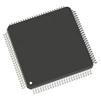
The BSVZ-210 tray packaging works well for prototype and qualification builds of the AD9430 in the 100-lead TQFP package with exposed thermal pad, which provides enhanced thermal dissipation compared to standard TQFP packages without the exposed pad. The exposed thermal pad requires proper thermal vias and soldering to the ground plane on the PCB for optimal thermal performance, which is critical for maintaining specifications in high-power applications running at 210 MSPS. We stock verified inventory with full lot traceability from the manufacturer to your facility, including documentation packages like Certificates of Conformity and material declarations that aerospace and defense contractors typically need for qualification processes. Anti-counterfeit inspection happens on every order to confirm authenticity, and we handle export compliance documentation for international shipments to defense contractors and aerospace manufacturers worldwide. The AD9430 evaluation board (AD9430/PCB) and supporting software tools like VisualAnalog are available for rapid prototyping and system characterization before committing to production volumes.
- 12-bit architecture with 210 MSPS sampling rate enabling high-resolution radar digitization
- 65 dB SNR and 80 dBc SFDR at 70 MHz for superior dynamic range
- 700 MHz full-power bandwidth supporting wideband radar and EW signal capture
- Excellent linearity with DNL = ±0.3 LSB and INL = ±0.5 LSB
- Flexible output options: demux CMOS (105 MSPS) or LVDS (210 MSPS)
- Single 3.3 V supply operation reducing power distribution complexity
- On-chip track-and-hold and reference simplifying system design
- Clock duty cycle stabilizer and out-of-range detection enhancing system reliability
- Industrial temperature range (−40°C to +85°C) for demanding aerospace environments
Frequently Asked Questions (FAQ)
What Is the Difference Between AD9430BSVZ-210 and AD9288BSTZ-80 for Radar Applications?
These two devices offer different performance characteristics optimized for distinct application requirements with significant differences in resolution, performance, power consumption, channel count, and package type. The AD9430 is a single 12-bit ADC consuming 1.3 W at 210 MSPS with 65 dB SNR and 80 dBc SFDR at 70 MHz input frequency, using a single 3.3 V supply in a 100-lead TQFP with exposed thermal pad. The AD9288 is a dual 8-bit ADC consuming 90 mW per channel (180 mW total) at 80 MSPS with 47 dB SNR and 70 dBc SFDR at 41 MHz, using a single 3.0 V supply in a 48-lead LQFP package. For radar and EW systems requiring high resolution with superior dynamic range and wider bandwidth, the AD9430 provides the necessary performance advantage with 12-bit resolution, 65 dB SNR, and 80 dBc SFDR. The 700 MHz full-power bandwidth enables IF sampling of signals up to 300 MHz, reducing system complexity compared to multi-stage downconversion architectures. For applications requiring dual-channel digitization at lower cost and power consumption where 8-bit resolution provides adequate dynamic range, the AD9288 offers significant power savings and provides independent operation of two channels for I/Q demodulation or diversity reception.
Does AD9430BSVZ-210 Support On-Chip Reference Voltage?
Yes, this device features an on-chip reference voltage source with scalable reference capability. The integrated reference eliminates the need for external reference components in many applications, reducing component count and board space requirements. The on-chip reference, combined with the track-and-hold circuit, simplifies system design and reduces overall bill of materials for radar receiver front ends and electronic warfare digitizers. For applications requiring different reference voltages or higher precision than the internal reference provides, external reference options can be implemented, though the integrated reference provides adequate performance for most aerospace and defense applications. The scalable reference architecture allows adjustment of reference voltage to optimize dynamic range for different input signal levels encountered in radar and EW systems.
What Is the Power Consumption of AD9430BSVZ-210 at 210 MSPS?
The device consumes 1.3 W typical at the maximum 210 MSPS conversion rate with the 3.3 V analog supply and appropriate digital driver supply voltage. This represents higher power consumption compared to 8-bit ADCs at lower sampling rates, which is expected given the significantly higher resolution (12 bits vs. 8 bits), faster sampling rate (210 MSPS vs. 80 MSPS), and wider bandwidth (700 MHz vs. 475 MHz). The 100-lead TQFP package with exposed thermal pad provides enhanced thermal dissipation compared to standard TQFP packages, which is critical for maintaining specifications in high-power applications running at 210 MSPS in tightly packed avionics chassis. Proper thermal design with thermal vias to the ground plane is required to ensure the device operates within its thermal limits and maintains specified performance characteristics.
Can AD9430BSVZ-210 Output Demultiplexed CMOS or LVDS Data?
Yes, this ADC supports two output data options providing flexibility in system architecture based on FPGA interface capabilities and system timing requirements. In demultiplexed CMOS mode, the ADC outputs 12-bit data on two ports at 105 MSPS each (half the 210 MSPS conversion rate), reducing output clock frequency requirements and simplifying timing closure in FPGA designs with slower IO standards. Each CMOS output port can be configured for 3.3 V or 2.5 V operation via the separate DRVDD supply pin. A data sync input ensures proper output data port alignment between the two demultiplexed ports, while a dedicated data clock output provides precise timing for FPGA capture logic. In LVDS mode, the ADC provides 12-bit data at the full 210 MSPS ENCODE clock rate through low-voltage differential signaling interfaces. LVDS outputs provide excellent noise immunity and reduced power consumption compared to CMOS outputs, critical for high-speed signal paths that run through long traces in avionics backplanes.
How Do I Request a Quote for ADI AD9430BSVZ-210?
Submit an inquiry through our website contact form or email our sales team directly. We will respond within 24 hours with pricing, availability, and lead time, and can discuss long-term supply agreements for radar and EW production programs requiring industrial-grade ADC components with full lot traceability and anti-counterfeit inspection.