
ACTEL AX2000-FG896M
- Axcelerator antifuse FPGA with 2,000,000 equivalent system gates and 21,504 logic cells
- 0.15µm 7-layer metal CMOS antifuse process — one-time programmable, SEU immune
- 649 MHz internal performance, 350+ MHz system performance at standard speed grade
- 896-pin FBGA package with up to 684 user I/O pins
- 295 Kbits embedded SRAM with integrated FIFO control logic and dual PLLs
- Military M-grade temperature range: –55°C to +125°C
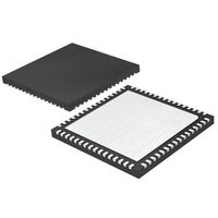
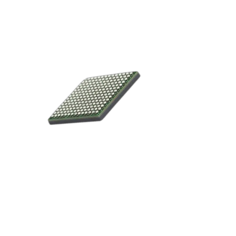
The ACTEL AX2000-FG896M is an Axcelerator family antifuse-based Field Programmable Gate Array (FPGA) from Actel (Microsemi / Microchip), delivering 2,000,000 equivalent system gates on Actel's advanced 0.15µm 7-layer metal CMOS antifuse process. The "FG896M" suffix identifies the 896-pin FBGA package and military M-grade temperature rating of –55°C to +125°C. As the highest I/O count variant of the AX2000 family, the AX2000-FG896M provides up to 684 user I/O pins — making it the preferred choice for military and aerospace designs requiring maximum gate density combined with the highest available pin count in the Axcelerator family.
Unlike SRAM-based FPGAs, the ACTEL AX2000-FG896M is nonvolatile and Live At Power-Up — no external configuration memory or boot device is required, and the device is inherently immune to single-event upsets (SEU) and firm errors. It features 295 Kbits of embedded SRAM with integrated FIFO control logic, dual PLLs, segmentable clock networks, chip-wide highway routing for deterministic high-speed timing, and FuseLock security technology to permanently prevent design readback and IP theft. Multi-standard I/O support including LVDS at 700 Mb/s, HSTL, SSTL, GTL+, and PCI/PCI-X with bank-selectable mixed-voltage operation at 1.5V, 1.8V, 2.5V, and 3.3V delivers the interface flexibility required for complex military system integration.
Related Products For Your Business

The ACTEL AX2000-FG896M combines the full 2-million-gate density of the Axcelerator family with the highest available I/O count — up to 684 user pins in a 896-pin FBGA package — qualified for military M-grade operation from –55°C to +125°C. For engineers evaluating the AX2000-FG896M datasheet, the 896-pin FBGA footprint makes this the go-to variant when both maximum logic capacity and maximum pin count are required in a single military-grade antifuse device. Built on a 0.15µm 7-layer metal process with 649 MHz internal performance, SEU immunity, and FuseLock security, it addresses the most demanding signal processing and I/O-intensive defense designs.
AX2000-FG896M Architecture: 2M Gates, 649 MHz, Axcelerator Antifuse
The ACTEL AX2000-FG896M is built on Actel’s 0.15µm 7-layer metal CMOS antifuse process, delivering 2,000,000 equivalent system gates and 21,504 SuperCluster logic cells with 649 MHz internal performance at standard speed grade. Its chip-wide highway routing provides deterministic, predictable timing closure across the full military temperature and voltage range — a critical advantage for high-reliability signal processing and communications designs. The device includes 295 Kbits of embedded SRAM with integrated FIFO control logic, dual on-chip PLLs for advanced clock management, and segmentable clock networks for efficient distribution across large, complex logic designs. FuseLock security technology permanently disables design readback and cloning after programming.
AX2000-FG896M Package and I/O: 896-Pin FBGA with 684 User I/Os
With up to 684 user I/O pins in a 896-pin FBGA package, the ACTEL AX2000-FG896M offers the widest I/O bandwidth in the Axcelerator family — enabling direct connection to high-pin-count memory, backplane, and multi-channel interface designs without external I/O expansion. Its bank-selectable mixed-voltage architecture supports 1.5V, 1.8V, 2.5V, and 3.3V I/O simultaneously, with full support for LVDS at 700 Mb/s, HSTL, SSTL2/3, GTL+, and PCI/PCI-X. The antifuse architecture ensures all 684 I/Os are permanently locked after programming with 100% pin locking capability, providing a stable, fully deterministic interface for deployed military systems.
Sourcing ACTEL AX2000-FG896M: Military Axcelerator FPGA with Maximum I/O
Defense and aerospace procurement teams sourcing the ACTEL AX2000-FG896M will find it among the most capable and sought-after legacy military antifuse FPGAs on the market, with long program lifecycles across active avionics, radar, and communications platforms. We maintain verified AX2000-FG896M inventory with full component traceability, certificate of conformance, and anti-counterfeit inspection for both urgent single-unit requirements and sustained long-term production agreements. Contact us today to confirm availability and request a competitive quote for the ACTEL AX2000-FG896M.
- The ACTEL AX2000-FG896M delivers 2,000,000 equivalent system gates on a 0.15µm 7-layer metal antifuse process.
- 21,504 SuperCluster logic cells with 649 MHz internal and 350+ MHz system performance at standard speed grade.
- Up to 684 user I/O pins — the highest I/O count available in the Axcelerator AX2000 family.
- One-time programmable antifuse architecture is SEU immune and inherently secure against configuration upset.
- FuseLock technology permanently prevents design readback, cloning, and reverse engineering.
- 295 Kbits of embedded SRAM with integrated FIFO control logic and dual on-chip PLLs.
- Bank-selectable mixed-voltage I/O at 1.5V, 1.8V, 2.5V, and 3.3V with LVDS at 700 Mb/s.
- 896-pin FBGA package rated for military M-grade operation at –55°C to +125°C.
- Live At Power-Up — no external boot device or configuration memory required.
- Urgent orders and long-term supply agreements for the ACTEL AX2000-FG896M are available upon request.
Frequently Asked Questions (FAQ)
What Is the ACTEL AX2000-FG896M and What Does It Do?
The ACTEL AX2000-FG896M is an Axcelerator family antifuse FPGA delivering 2,000,000 equivalent system gates at 649 MHz internal performance, with up to 684 user I/O pins, 295 Kbits of embedded SRAM, dual PLLs, and FuseLock security in a 896-pin FBGA package, rated for military M-grade operation from –55°C to +125°C.
How Does the ACTEL AX2000-FG896M Differ From the AX2000-CQ256M?
Both devices share the same 2M gate AX2000 die and Axcelerator antifuse architecture, but differ significantly in package and I/O count. The AX2000-FG896M provides up to 684 user I/O pins in a 896-pin FBGA package, compared to the CQ256M’s smaller ceramic CQFP footprint with fewer available I/Os — making the FG896M the preferred choice for high pin count system designs.
Is the ACTEL AX2000-FG896M SEU Immune?
Yes. The antifuse architecture of the ACTEL AX2000-FG896M is inherently immune to single-event upsets (SEU) and firm errors caused by high-energy particle strikes, making it a trusted choice for space, avionics, and radiation-exposed military environments where SRAM-based FPGAs are vulnerable to configuration corruption.
What Is the Operating Temperature Range of the ACTEL AX2000-FG896M?
The ACTEL AX2000-FG896M is rated for military M-grade operation from –55°C to +125°C, suitable for the full range of airborne, shipboard, and ground-based military platform environments.
How Do I Order the ACTEL AX2000-FG896M?
You can submit an inquiry directly through our website contact form or email our sales team. We will respond with pricing, lead time, and availability within 24 hours for the ACTEL AX2000-FG896M.