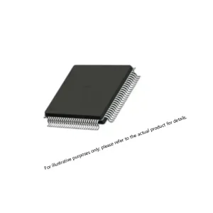
ADI LTC2209IUP#PBF
- 16-bit resolution at 160Msps sample rate with 700MHz full-power input bandwidth sample-and-hold
- 77.3dBFS noise floor, 100dB SFDR, and 70fsRMS ultra-low aperture jitter for high-IF undersampling
- Selectable LVDS or CMOS parallel output with optional demultiplexed half-rate bus and data randomizer
- PGA front end supporting 2.25VP-P or 1.5VP-P input ranges; optional internal dither for improved SFDR
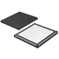
- Single 3.3V supply, 1.53W power dissipation, 64-pin 9mm × 9mm QFN package, −40°C to +85°C
Modern radar, electronic warfare, and wideband signal intelligence receivers demand analog-to-digital converters capable of digitizing signals at intermediate frequencies well above the Nyquist band, while maintaining the dynamic range necessary to detect weak targets in the presence of strong interferers. Conventional ADCs with limited spurious-free dynamic range or high aperture jitter introduce noise floors and spurious tones that mask low-level signals and degrade probability of detection. As receiver architectures migrate toward direct RF sampling and wideband digital signal processing, the ADC becomes the critical performance bottleneck in the entire receive chain.
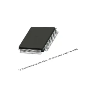
The ADI LTC2209IUP#PBF is a 16-bit, 160Msps pipeline ADC optimized for high-frequency, wide dynamic range signal digitization. With a 700MHz full-power bandwidth sample-and-hold, 77.3dBFS noise floor, 100dB SFDR, and 70fsRMS aperture jitter, it supports direct undersampling of signals up to 700MHz without an analog downconversion stage, significantly reducing system complexity in radar front-ends and EW receivers. The IUP variant is housed in a compact 64-pin 9mm × 9mm QFN package, operates from a single 3.3V supply at 1.53W, and covers the −40°C to +85°C industrial temperature range. Flexible digital outputs — selectable LVDS or CMOS, full-rate or demultiplexed half-rate — and a programmable PGA front end make the LTC2209 directly interfaceable with FPGAs and DSPs in high-density signal processing subsystems.
Related Products For Your Business
The ADI LTC2209IUP#PBF is a 16-bit, 160Msps high-speed pipeline ADC from Analog Devices, delivering 77.3dBFS noise floor, 100dB SFDR, and 70fsRMS aperture jitter in a 64-pin 9mm × 9mm QFN package. Its 700MHz full-power input bandwidth enables direct undersampling of L-, S-, and C-band IF signals without analog downconversion, making it the preferred ADC for radar, electronic warfare, and wideband digital receiver design. Operating from a single 3.3V supply at 1.53W, the LTC2209IUP#PBF is pin-compatible with the LTC2208 (130Msps) and LTC2217 (105Msps), enabling drop-in rate scaling across the same PCB layout.
For reference against related high-speed ADCs in our inventory:
| Product | Resolution | Sample Rate | SFDR | Supply | Package |
|---|---|---|---|---|---|
| LTC2209IUP#PBF | 16-bit | 160 Msps | 100 dB | 3.3 V | 64-QFN |
| LTC2207IUP#PBF | 16-bit | 130 Msps | 100 dB | 3.3 V | 48-QFN |
| AD9689BBPZ-2000 | 14-bit | 2000 Msps | — | 1.8 V | BGA |
Military-Grade Performance & Reliability
Manufactured by Analog Devices under its industry-leading quality program targeting zero defective parts per million, the LTC2209IUP#PBF is the industrial-temperature-range variant (−40°C to +85°C) of the LTC2209 family, fully characterized over temperature with guaranteed AC and DC specifications. The 70fsRMS aperture jitter is critical in radar and EW applications: at 200MHz input frequency, this jitter level contributes less than 0.5dBFS SNR degradation, preserving the full 16-bit dynamic range for signal detection and classification tasks. The optional internal dither feature improves SFDR by randomizing ADC nonlinearities, particularly beneficial in narrowband EW and spectrum monitoring applications. The clock duty cycle stabilizer maintains full-speed performance across a wide range of clock signal types and duty cycles, simplifying system clock distribution design.
Supply Chain & Quality Assurance
The LTC2209IUP#PBF is an Analog Devices product (formerly Linear Technology), available through the global ADI authorized distribution network including DigiKey, Mouser, Arrow, and Avnet. The #PBF suffix designates RoHS-compliant lead-free packaging per ADI’s lead-free program. As a specialist distributor for high-performance ADI signal chain components, we stock the LTC2209IUP#PBF with full factory traceability: ADI certificates of conformance, date code records, and ESD/MSL-compliant packaging. All parts are inspected for authenticity and condition prior to shipment, with anti-counterfeit measures aligned to AS6081 best practices.
Selection Guide & Application Notes
The LTC2209IUP#PBF (−40°C to +85°C, industrial) is the standard production variant for defense and commercial system integration. For wider temperature coverage, consult ADI for extended temperature options. The PGA input range should be matched to the system’s maximum input signal level: the 2.25VP-P range maximizes SNR for baseband and low-IF applications, while the 1.5VP-P range improves SFDR above 100MHz — the preferred setting for radar IF and EW receiver designs. Drive the differential analog input with a high-performance ADC driver such as the LTC6417 (1.6GHz bandwidth) or equivalent. For FPGA interfacing in LVDS mode, route differential output pairs with matched trace lengths and ensure OVDD is independently decoupled. The demultiplexed half-rate CMOS output mode reduces FPGA I/O pin count by 50%, simplifying routing in high-density ADC array designs.
FAQ
What does LTC2209IUP#PBF mean?
LTC2209 = 16-bit 160Msps ADC product family; I = industrial temperature grade (−40°C to +85°C); UP = 64-lead QFN package; #PBF = RoHS-compliant lead-free finish (Pb-Free).
What is the maximum analog input frequency the LTC2209IUP#PBF can digitize?
The sample-and-hold has 700MHz full-power bandwidth, enabling direct undersampling of IF signals up to 700MHz. SFDR exceeds 84dB at 250MHz input with the 1.5VP-P input range setting.
LVDS or CMOS output — which should I use for radar/EW designs?
LVDS is preferred for radar and EW designs: it provides lower output noise, better EMI performance, and higher switching speed. CMOS is suitable for lower-frequency FPGA interfaces where LVDS transceivers are unavailable or power-constrained.
What is the significance of 70fsRMS aperture jitter?
At 200MHz input, 70fsRMS jitter contributes approximately 0.4dBFS SNR degradation — negligible for 16-bit dynamic range. This enables the LTC2209 to undersample high-IF signals while maintaining the full noise floor required for radar target detection.
Is the LTC2209IUP#PBF pin-compatible with other ADCs in the family?
Yes. It is pin-compatible with the LTC2208 (130Msps) and LTC2217 (105Msps), allowing direct rate scaling on the same PCB without layout changes — a significant advantage for multi-variant radar and EW platform development.
What clock source is recommended for optimal SFDR performance?
A low-phase-noise differential clock source is strongly recommended. Drive ENC+/ENC− with a bandpass-filtered sinusoidal signal or a low-jitter PECL/LVDS clock. The optional clock duty cycle stabilizer relaxes duty cycle requirements, but a clean, low-jitter source remains the primary determinant of achievable SFDR at high input frequencies.