
ADI LTC2207IUK#PBF
- 16-bit resolution with 105Msps sampling rate
- 78.2dBFS noise floor and 100dB SFDR performance
- 2.25VP-P or 1.5VP-P selectable input range
- 700MHz full-power bandwidth sample-and-hold amplifier
- Single 3.3V power supply with 900mW typical power dissipation
Related Products For Your Business
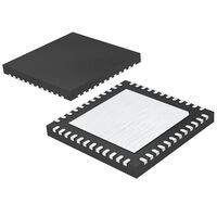
The ADI LTC2207IUK#PBF is a 16-bit, 105Msps pipeline ADC from Analog Devices, delivering 77.9dBFS SNR, 100dB SFDR, and 80fsRMS aperture jitter in a compact 48-pin 7mm × 7mm QFN package. Operating from a single 3.3V supply at 900mW, it is the lowest-power member of the pin-compatible LTC220x family that achieves 100dB SFDR, making it the preferred choice for multi-channel and SWaP-constrained radar and EW receiver architectures. Its 700MHz full-power input bandwidth supports direct undersampling of L- and S-band intermediate frequencies, eliminating one analog downconversion stage and reducing receiver chain complexity.
For reference against related high-speed ADCs in our inventory:
| Product | Resolution | Sample Rate | SNR | Power | Package |
|---|---|---|---|---|---|
| LTC2207IUK#PBF | 16-bit | 105 Msps | 77.9 dB | 900 mW | 48-QFN |
| LTC2209IUP#PBF | 16-bit | 160 Msps | 77.3 dB | 1,530 mW | 64-QFN |
| AD9689BBPZ-2000 | 14-bit | 2,000 Msps | — | — | BGA |
Military-Grade Performance & Reliability
Manufactured under ADI’s zero-defect quality program, the LTC2207IUK#PBF is fully characterized over the −40°C to +85°C industrial temperature range with guaranteed AC and DC specifications. The 80fsRMS aperture jitter maintains sub-0.5dBFS SNR degradation at input frequencies up to 200MHz, preserving 16-bit dynamic range integrity for pulse detection and emitter classification in EW receivers. The optional internal dither circuit randomizes ADC nonlinearities, extending effective SFDR beyond 100dBc for low-level narrowband input signals — a critical feature for ELINT receivers detecting weak emitters against a strong interference background. Pin compatibility with the LTC2206 (80Msps), LTC2208 (130Msps), and LTC2209 (160Msps) enables scalable multi-rate receiver platform design from a single PCB layout, significantly reducing NRE cost across program variants.
Supply Chain & Quality Assurance
The LTC2207IUK#PBF is an Analog Devices product available through the global ADI authorized distribution network including DigiKey, Mouser, Arrow, and Avnet. The IUK suffix designates the industrial temperature grade in the 48-pin QFN package; #PBF confirms RoHS-compliant lead-free packaging. We stock this part with full factory traceability — ADI certificates of conformance, date code records, and ESD/MSL-compliant packaging — with anti-counterfeit inspection aligned to AS6081 best practices on every order.
Selection Guide & Application Notes
The LTC2207IUK#PBF is optimal for multi-channel receiver designs where per-channel power must remain below 1W and PCB area is constrained. For higher sample rate requirements on the same footprint, evaluate the LTC2208 (130Msps, 64-QFN) or LTC2209 (160Msps, 64-QFN) — both share insert-arrangement compatibility. Set the PGA input range to 1.5VP-P for IF inputs above 100MHz to optimize SFDR; use 2.25VP-P for baseband applications maximizing SNR. Drive ENC+/ENC− differentially with a low-phase-noise clock source; the optional duty cycle stabilizer relaxes clock quality requirements in less demanding applications. For FPGA interfacing, route LVDS output pairs with matched lengths and decouple OVDD independently from VDD.
FAQ
What does LTC2207IUK#PBF mean?
LTC2207 = 16-bit 105Msps ADC; I = industrial temperature (−40°C to +85°C); UK = 48-lead QFN package (7mm × 7mm); #PBF = RoHS-compliant lead-free finish.
How does the LTC2207IUK#PBF differ from the LTC2209IUP#PBF?
The LTC2207 operates at 105Msps in a 48-pin QFN at 900mW; the LTC2209 runs at 160Msps in a 64-pin QFN at 1,530mW. Both achieve 100dB SFDR and are pin-compatible at the circuit level, enabling sample-rate scaling with minimal redesign effort.
What is the maximum analog input frequency this ADC can handle?
The sample-and-hold provides 700MHz full-power bandwidth, supporting direct undersampling of L- and S-band IF signals. SFDR remains at 100dB through the baseband region, with optimized performance when using the 1.5VP-P input range above 100MHz.
Why choose the 48-QFN (UK) package over the 64-QFN (UP)?
The 48-QFN (7mm × 7mm) is significantly smaller and more power-efficient, making it the preferred choice for multi-channel receiver boards and SWaP-constrained platforms. The 64-QFN UP package supports LVDS outputs required at 130Msps and above; at 105Msps the LTC2207 UK package provides CMOS or LVDS output with adequate I/O bandwidth.
Does internal dither improve performance in EW receiver designs?
Yes. The internal dither circuit randomizes ADC harmonic and spurious content, effectively extending SFDR beyond 100dBc for low-level narrowband input signals. This is particularly valuable in ELINT and COMINT receivers where weak emitter signals must be resolved against a strong interference floor.
Is this part pin-compatible with other LTC220x ADCs?
Yes. The LTC2207 is pin-compatible with the LTC2206 (80Msps) and shares the same 48-pin QFN footprint, allowing direct speed-grade substitution. The LTC2208 (130Msps) and LTC2209 (160Msps) use a 64-pin QFN but maintain circuit-level interface compatibility, enabling scalable platform designs from a common schematic.