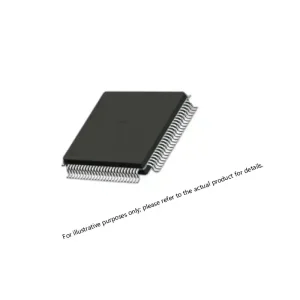

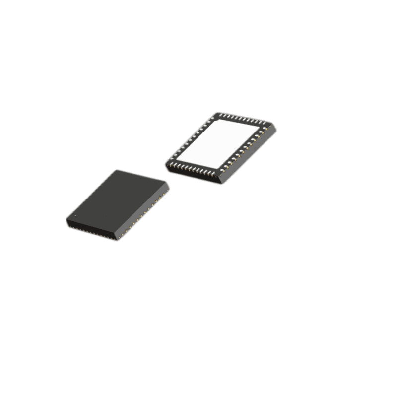

ADI LTC2165IUK#PBF
- 16-bit resolution at 125Msps with 550MHz full-power input bandwidth and 70fsRMS aperture jitter for IF undersampling
- 76.8dB SNR and 90dB SFDR with selectable 1VP-P to 2VP-P input range via SPI-programmable reference
- Full-rate CMOS, DDR CMOS, or DDR LVDS digital outputs with optional data randomizer and clock duty cycle stabilizer
- SPI serial programming port for flexible configuration of output mode, power-down, nap, and shutdown states
- Single 1.8V supply, ultra-low 194mW power dissipation, 48-pin 7mm × 7mm QFN, −40°C to +85°C industrial grade
_*]:min-w-0 gap-3">
Portable electronic warfare systems, compact airborne radar pods, and multi-channel SIGINT receivers impose increasingly stringent power budgets on their ADC subsystems. As digital receiver architectures move toward higher channel counts and tighter SWaP envelopes, power dissipation per ADC channel becomes a primary design constraint — often more critical than raw sample rate. Conventional high-performance ADCs achieving 100dB SFDR at comparable speeds typically dissipate 800mW to 1.5W per channel, making them unsuitable for battery-powered or thermally constrained platforms without active cooling.
_*]:min-w-0 gap-3">
The ADI LTC2165IUK#PBF addresses this constraint directly as a 16-bit, 125Msps pipeline ADC operating from a single 1.8V supply at just 194mW — roughly one-fifth the power of comparable 3.3V ADCs at similar sample rates. With 76.8dB SNR, 90dB SFDR, and 70fsRMS aperture jitter, it delivers the dynamic range and IF undersampling capability required for radar warning receivers, EW monitoring systems, and multi-channel spectrum surveillance platforms where per-channel power must remain below 200mW. Flexible DDR CMOS or DDR LVDS digital outputs, an SPI configuration port, and built-in shutdown and nap power modes further optimize system-level power management in duty-cycled radar and communications receiver architectures.
Related Products For Your Business
The ADI LTC2165IUK#PBF is a 16-bit, 125Msps low-power pipeline ADC from Analog Devices, delivering 76.8dB SNR and 90dB SFDR from a single 1.8V supply at just 194mW — approximately one-fifth the power of comparable 3.3V ADCs at similar sample rates. Its 550MHz full-power input bandwidth and 70fsRMS aperture jitter support IF undersampling of signals up to the UHF band, making it the preferred choice for SWaP-constrained radar warning receivers, portable EW systems, and multi-channel spectrum surveillance platforms where per-channel power must remain below 200mW. Pin-compatible speed grades of 105Msps (LTC2164) and 80Msps (LTC2163) enable scalable multi-rate platform design from a single PCB layout.
For reference against related high-speed ADCs in our inventory:
| Product | Resolution | Sample Rate | SNR | Supply | Power |
|---|---|---|---|---|---|
| LTC2165IUK#PBF | 16-bit | 125 Msps | 76.8 dB | 1.8 V | 194 mW |
| LTC2207IUK#PBF | 16-bit | 105 Msps | 77.9 dB | 3.3 V | 900 mW |
| LTC2209IUP#PBF | 16-bit | 160 Msps | 77.3 dB | 3.3 V | 1,530 mW |
Military-Grade Performance & Reliability
Manufactured under ADI’s zero-defect quality program, the LTC2165IUK#PBF is fully characterized over the −40°C to +85°C industrial temperature range with guaranteed AC and DC specifications across supply and temperature corners. The 70fsRMS aperture jitter enables IF undersampling with less than 0.4dBFS SNR degradation at 100MHz input — preserving effective 16-bit dynamic range for threat classification and pulse characterization in EW receiver chains. The SPI configuration port enables runtime control of output mode, input range, and power state, supporting duty-cycled receiver architectures where the ADC is powered down between receive windows to reduce average dissipation below 194mW. Built-in shutdown and nap modes offer a hierarchy of power reduction, from partial standby (nap) to full power-off (shutdown), with fast wake-up to minimize blind time in pulsed radar and intermittent receive applications.
Supply Chain & Quality Assurance
The LTC2165IUK#PBF is an Analog Devices product (formerly Linear Technology), available through the global ADI authorized distribution network including DigiKey, Mouser, Arrow, and Avnet. The IUK suffix designates the industrial temperature grade in the 48-pin QFN package; #PBF confirms RoHS-compliant lead-free packaging. We stock this part with full factory traceability — ADI certificates of conformance, date code records, and ESD/MSL-compliant packaging — with anti-counterfeit inspection aligned to AS6081 best practices on every order.
Selection Guide & Application Notes
The LTC2165IUK#PBF (125Msps) is the highest-speed variant of the pin-compatible LTC216x low-power family; LTC2164 (105Msps, ~163mW) and LTC2163 (80Msps, ~108mW) offer further power reduction at lower sample rates on the same footprint. Set the input range via the SENSE pin or SPI register: the 2VP-P range maximizes SNR for baseband applications, while the 1VP-P range improves SFDR at higher IF input frequencies. The DDR LVDS output mode halves the required FPGA I/O pin count versus full-rate CMOS at 125Msps, simplifying high-density multi-channel board design. Drive ENC+/ENC− differentially with a low-phase-noise source; the optional duty cycle stabilizer relaxes clock quality requirements in less noise-sensitive applications. Decouple OVDD independently from VDD using 100nF ceramic capacitors placed within 1mm of each supply pin.
FAQ
What does LTC2165IUK#PBF mean?
LTC2165 = 16-bit 125Msps low-power ADC; I = industrial temperature grade (−40°C to +85°C); UK = 48-lead QFN package (7mm × 7mm); #PBF = RoHS-compliant lead-free finish.
How does the LTC2165IUK#PBF compare to the LTC2207IUK#PBF in power and performance?
The LTC2165 operates at 1.8V consuming 194mW; the LTC2207 requires 3.3V at 900mW — nearly 4.6× higher power. The LTC2207 achieves slightly better SNR (77.9dB vs 76.8dB) and higher SFDR (100dB vs 90dB). The LTC2165 is the clear choice for battery-powered or thermally constrained platforms; the LTC2207 suits fixed-power applications demanding maximum dynamic range.
What output modes are available and which is best for FPGA interfacing?
Three modes are available: full-rate CMOS, DDR CMOS, and DDR LVDS. DDR LVDS is recommended for FPGA designs at 125Msps — it halves the required I/O pin count versus full-rate CMOS while providing lower EMI and better noise immunity. Full-rate CMOS suits lower sample rates or FPGAs without LVDS receivers.
Can the LTC2165 undersample IF signals above its Nyquist frequency?
Yes. The 550MHz full-power bandwidth sample-and-hold supports direct undersampling of IF signals well above the 62.5MHz Nyquist limit, aliasing them into the baseband with 70fsRMS jitter contributing minimal SNR degradation. This enables second-, third-, and higher-Nyquist-zone reception without analog downconversion.
What power management modes are available for duty-cycled systems?
Two modes are available: nap mode for partial standby with fast wake-up, and shutdown for full power-off. Both are SPI-programmable, enabling runtime power state control. This is particularly valuable in pulsed radar and EW receive windows where the ADC can be placed in nap between pulses, reducing average power well below the 194mW continuous rating.
Is the LTC2165IUK#PBF pin-compatible with slower speed-grade variants?
Yes. The LTC2164 (105Msps) and LTC2163 (80Msps) are pin-compatible with the LTC2165 in the same 48-pin QFN package, allowing direct speed-grade selection on a common PCB layout. This enables a single board design to be qualified across multiple performance and power tiers for different platform variants.