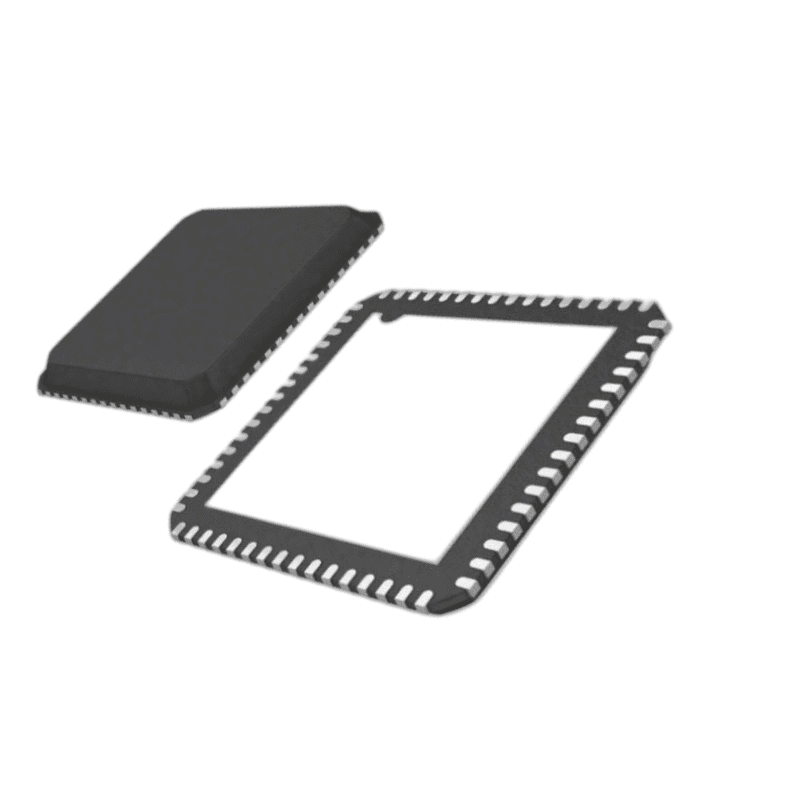
ADI AD9269BCPZ-80
- SNR = 77.6 dBFS (9.7 MHz) and SFDR = 93 dBc (9.7 MHz) at 80 MSPS conversion rate
- 1.8 V analog supply operation with flexible 1.8 V to 3.3 V output supply
- 700 MHz full-power bandwidth with 2 V p-p differential analog input
- Integrated quadrature error correction (QEC) for direct conversion receiver applications
- Integer 1-to-6 input clock divider with optional duty cycle stabilizer for consistent performance
Related Products For Your Business
The AD9269BCPZ-80 provides dual 16-bit 80 MSPS ADC performance optimized for aerospace radar and electronic warfare applications where high dynamic range and integrated quadrature error correction determine system effectiveness. You get 77.6 dBFS SNR and 93 dBc SFDR at 9.7 MHz with a 700 MHz full-power bandwidth that handles IF signals up to 200 MHz without intermediate downconversion stages. This dual ADC operates from a single 1.8 V analog supply with separate digital output driver support for both 1.8 V and 3.3 V CMOS interfaces, giving you flexibility in system timing and EMI management. The integrated programmable voltage reference and 1-to-6 input clock divider simplify board-level design while maintaining excellent jitter performance through the on-chip duty cycle stabilizer.
Dual-Channel Pipeline ADC Architecture with Quadrature Error Correction
Two independent 16-bit ADC channels digitize at 80 MSPS through a multistage differential pipelined architecture with integrated output error correction. Direct IF sampling at frequencies up to 200 MHz converts intermediate frequency signals straight to digital format, skipping the extra downconversion stages that would otherwise add components to your signal chain. The 700 MHz full-power bandwidth enables capture of wideband radar returns and electronic warfare signals with minimal signal degradation. The integrated quadrature error correction (QEC) block corrects for DC offset, gain, and phase mismatch between the two channels, which is critical for I/Q demodulation systems where channel balance affects beamforming performance in phased array radar systems. Programmable QEC bandwidth control allows fine-tuning for specific application requirements.
AD9269BCPZ-80 vs AD9268BCPZ-80: QEC and Performance Comparison
Pin-compatible dual ADC options from Analog Devices offer different feature sets optimized for specific application requirements. The comparison table below shows the key differences between the AD9269 with integrated QEC and the AD9268 without QEC.
| Parameter | AD9269BCPZ-80 (16-Bit Industrial with QEC) | AD9268BCPZ-80 (16-Bit Industrial) |
|---|---|---|
| Resolution | 16 bits | 16 bits |
| Channels | Dual (2) | Dual (2) |
| Sampling Rate | 80 MSPS | 80 MSPS |
| SNR (at 9.7 MHz) | 77.6 dBFS | 78.2 dBFS |
| SFDR (at 9.7 MHz) | 93 dBc | 88 dBc |
| IF Sampling Frequency | Up to 200 MHz (optimal) | Up to 300 MHz |
| Full-Power Bandwidth | 700 MHz | 650 MHz |
| Power Consumption | 100 mW per channel (200 mW total) at 80 MSPS | 750 mW (both channels) at 80 MSPS |
| Quadrature Error Correction | Integrated (DC offset, gain, phase) | Not available |
| Input Voltage Range | 2 V p-p differential | 1 V p-p to 2 V p-p differential |
| Clock Divider | Integer 1-to-6 | Integer 1-to-8 |
| Output Supply | 1.8 V to 3.3 V CMOS | 1.8 V CMOS or LVDS |
| Package | 64-Lead LFCSP BCPZ-80 (Tray) | 64-Lead LFCSP BCPZ-80 (Tray) |
| Operating Temperature | −40°C to +85°C (Industrial) | −40°C to +85°C (Industrial) |
| Best Application Fit | Direct Conversion Receivers & I/Q Demodulation | Radar & EW with High IF Sampling |
If your application requires integrated quadrature error correction for direct conversion receivers or I/Q demodulation systems, the AD9269 provides the necessary channel balance correction while maintaining excellent dynamic range. For applications requiring higher IF sampling frequencies up to 300 MHz or LVDS output interfaces, the AD9268 offers superior bandwidth and interface flexibility. Both devices maintain the same 64-lead LFCSP form factor and pinout, enabling easy migration between QEC-enabled and non-QEC variants based on system requirements. For complete transceiver integration with both transmit and receive functionality in a single device, the AD9176BBPZ and AD9081BBPZ-4D4AC handle both sides of the signal chain.
Sourcing ADI AD9269BCPZ-80 with Industrial Grade Validation
The BCPZ-80 tray packaging works well for prototype and qualification builds of the AD9269 in the 64-lead LFCSP package, and the BCPZRL7 tape-and-reel variant is available when you move into production volumes that need automated assembly. We stock verified inventory with full lot traceability from the manufacturer to your facility, including documentation packages like Certificates of Conformity and material declarations that aerospace and defense contractors typically need for qualification processes. Anti-counterfeit inspection happens on every order to confirm authenticity, and we handle export compliance documentation for international shipments to defense contractors and aerospace manufacturers worldwide. The AD9269 evaluation board (AD9269-80EBZ) and supporting software tools are available for rapid prototyping and system characterization before committing to production volumes.
- Dual 16-bit architecture with 80 MSPS sampling rate enabling high-resolution radar digitization
- Integrated quadrature error correction (QEC) for DC offset, gain, and phase mismatch correction
- Direct IF sampling up to 200 MHz eliminates intermediate downconversion stages
- 700 MHz full-power bandwidth supporting wideband radar and EW signal capture
- Integer 1-to-6 input clock divider enabling flexible clock architecture design
- Duty cycle stabilizer maintaining consistent performance across clock variations
- Separate digital driver supply accommodating both 1.8 V and 3.3 V CMOS interfaces
- Data output multiplexing option for single-bus output configurations
Frequently Asked Questions (FAQ)
What Is the Difference Between AD9269BCPZ-80 and AD9268BCPZ-80 for Radar Applications?
These two devices are pin-compatible dual ADCs from the same Analog Devices product family, differing primarily in feature optimization for specific application scenarios. The AD9269 incorporates an integrated quadrature error correction (QEC) block that corrects for DC offset, gain, and phase mismatch between the two channels, making it ideal for direct conversion receivers and I/Q demodulation systems where channel balance is critical. It provides 77.6 dBFS SNR and 93 dBc SFDR at 9.7 MHz input frequency with 700 MHz bandwidth and 100 mW per channel power consumption at 80 MSPS. The AD9268 does not include QEC but offers higher IF sampling capability up to 300 MHz, 78.2 dBFS SNR, 88 dBc SFDR, and LVDS output interface support. For radar and EW systems requiring I/Q demodulation with automated channel mismatch correction, the AD9269 provides the necessary QEC functionality, while the AD9268 is better suited for applications requiring higher IF frequencies or LVDS interfaces.
Does AD9269BCPZ-80 Support Quadrature Error Correction (QEC)?
Yes, this device features an integrated quadrature error correction (QEC) block that corrects for DC offset, gain, and phase mismatch between the two ADC channels. The QEC functionality is programmable through the SPI interface, allowing users to adjust DC offset, gain, and phase correction parameters with programmable bandwidth control for each correction type. This feature is particularly beneficial for direct conversion receivers and I/Q demodulation systems in radar and electronic warfare applications where channel imbalance can degrade beamforming performance in phased array systems. The QEC block can be enabled or disabled as needed, and the correction parameters can be frozen once optimal settings are determined for stable operation.
What Is the Power Consumption of AD9269BCPZ-80 at 80 MSPS?
The device consumes 100 mW per channel (200 mW typical total for both channels) when operating at the maximum 80 MSPS conversion rate with the 1.8 V analog supply and 1.8 V digital driver supply. This represents significantly lower power consumption compared to the AD9268 at the same sampling rate, making the AD9269 well-suited for power-constrained aerospace and defense applications. Flexible power-down options allow significant power savings when desired, including individual channel power-down for applications where fewer than two channels are continuously required. The separate digital driver supply enables additional power optimization by selecting the appropriate voltage for 1.8 V or 3.3 V CMOS operation.
Can AD9269BCPZ-80 Operate with 3.3 V CMOS Outputs?
Yes, this dual ADC supports both 1.8 V and 3.3 V CMOS output interfaces through the separate DRVDD digital output driver supply. The 3.3 V CMOS mode provides traditional parallel output compatibility with existing FPGA and processor interfaces that operate at higher voltage levels, while the 1.8 V CMOS mode offers reduced power consumption for low-power avionics systems. The output data format is configurable through the SPI interface to support offset binary, twos complement, or gray coding, enabling flexible interfacing with various digital processing platforms used in aerospace and defense systems. Additionally, output data can be multiplexed onto a single output bus for designs requiring reduced pin count.
How Do I Request a Quote for ADI AD9269BCPZ-80?
Submit an inquiry through our website contact form or email our sales team directly. We will respond within 24 hours with pricing, availability, and lead time, and can discuss long-term supply agreements for radar and EW production programs requiring industrial-grade ADC components with full lot traceability and anti-counterfeit inspection.