
ADI 5962 9689202VJA(AD565ATD)
- High-speed 12-bit current-steering DAC — 250 ns maximum settling to ±½ LSB, 35 ns full-scale switching
- Laser wafer trimmed thin-film resistors — ±¼ LSB maximum linearity (T grade), monotonicity guaranteed over temperature
- On-chip buried Zener reference with 10 ppm/°C typical full-scale gain temperature coefficient
- Flexible output configurations: unipolar 0V to +10V, bipolar ±5V or ±10V — no external DAC required
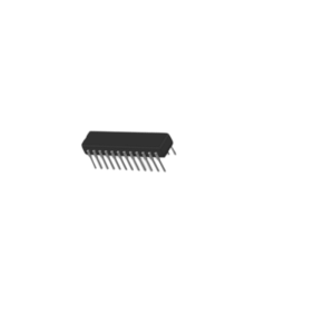
- MIL-STD-883B qualified under SMD 5962-96892 — 24-lead ceramic DIP package
- Military temperature range: –55°C to +125°C
Speed and precision rarely coexist in the same DAC without cost tradeoffs. The ADI 5962-9689202VJA — the military SMD designation for Analog Devices' AD565ATD processed to MIL-STD-883B — achieves both in a single 24-lead ceramic DIP package. At 250 ns maximum settling to ±½ LSB and a full-scale switching time under 35 ns, it operates at conversion speeds that most precision 12-bit DACs cannot approach, while the laser wafer trimmed thin-film resistor network delivers ±¼ LSB maximum linearity across the full –55°C to +125°C military temperature range. The T grade specified by this SMD designation is the tightest available, with linearity guaranteed overtemperature — not just at 25°C.
The AD565A architecture centers on 12 precision bipolar current-steering switches driven by a control amplifier and a laser-trimmed R-2R resistor network, with an on-chip buried Zener reference whose absolute value and temperature coefficient are laser-trimmed simultaneously — a process that achieves a typical full-scale gain TC of 10 ppm/°C without external adjustment. Unipolar and bipolar output configurations are pin-selectable, covering 0V to +10V, ±5V, and ±10V ranges with appropriate external resistor connections. For military system designers evaluating the 5962-9689202VJA, the combination of sub-microsecond settling, overtemperature linearity guarantee, and on-chip reference eliminates the discrete component count that competing high-speed DAC solutions require.
Related Products For Your Business
Two hundred and fifty nanoseconds to ±½ LSB — that settling specification defines the AD565A’s market position in military DAC design. For radar, electronic warfare, and high-speed waveform generation applications where the DAC must settle within a fraction of a microsecond to maintain timing margins, the 5962-9689202VJA delivers a qualified solution that does not require trading precision for speed. The T grade under SMD 5962-96892 guarantees ±¼ LSB linearity overtemperature — the same tightness required for precision applications — in a device that also switches at 35 ns full-scale transitions. The on-chip buried Zener reference, laser-trimmed to 10 ppm/°C typical gain TC, rounds out a genuinely complete high-speed DAC solution in a single military-qualified component.
5962-9689202VJA Architecture: Bipolar Current-Steering for Sub-Microsecond Settling
The AD565A’s speed comes from its bipolar current-steering architecture — unlike CMOS R-2R ladders that switch voltage through finite impedances, the bipolar switches steer pre-established currents between output nodes with transition times governed by transistor switching rather than RC charging. Twelve precision switches, each controlling a binary-weighted current fraction from the buried Zener reference, produce the output current word with the predictability that laser-trimmed thin-film resistor ratios provide. The control amplifier that drives the switches is designed specifically for minimum glitch energy during code transitions — a specification that matters in radar and EW applications where DAC glitch area directly contributes to spurious spectral content. The output current can be converted to voltage in unipolar or bipolar configurations using the on-chip span resistors and an external op amp, with the buried Zener supplying both the reference current and the bipolar offset current in bipolar mode.
5962-9689202VJA vs Other Military 12-Bit and 16-Bit DAC Options
Speed grade selection often drives the choice between the AD565A and slower, higher-resolution alternatives in military signal chain design:
| 5962-9689202VJA (AD565AT) | 5962-9475501MPA (AD7846S) | 5962-9684601QLA (AD660S) | |
|---|---|---|---|
| Resolution | 12-bit | 16-bit | 16-bit |
| Settling Time | 250 ns to ±½ LSB | 10 µs to ½ LSB | 10 µs to ½ LSB |
| Architecture | Bipolar current-steering | Segmented voltage | BiMOS II current-steering |
| On-chip Reference | Yes (buried Zener) | No | Yes (10V Zener) |
| Interface | Parallel (direct bit) | 16-bit parallel + readback | Serial / 2×8-bit byte |
| Best For | High-speed waveform, radar, EW | Precision control, closed-loop | Multi-DAC serial chains |
The 5962-9689202VJA is the correct choice when settling speed is the primary specification — radar update rates, EW waveform generation, and high-speed ATE stimulus applications where the DAC must settle within hundreds of nanoseconds. For precision closed-loop control or ATE where accuracy and voltage range flexibility outweigh settling speed, the AD7846 or AD660 alternatives address those requirements.
Sourcing the ADI 5962-9689202VJA
The AD565A in its military ceramic package remains specified in active defense programs where its combination of sub-microsecond settling and overtemperature linearity guarantee is difficult to replace with a qualified alternative. We maintain verified inventory with full lot traceability, MIL-STD-883B certificate of conformance, and anti-counterfeit inspection on every order. Contact us today to confirm availability and request a quote — our team responds within 24 hours.
- T grade guarantees ±¼ LSB linearity overtemperature — not just at 25°C
- 35 ns full-scale switching time enables DAC update rates well into the megahertz range
- On-chip buried Zener reference laser-trimmed for both absolute value and temperature coefficient simultaneously
- Bipolar current-steering architecture minimizes glitch energy during code transitions
- Output span resistors included on-chip — unipolar and bipolar configurations need only external op amp
- Short-circuit protected reference output — available for external use without risk of device damage
- 24-lead ceramic DIP package — hermetic construction for military environmental reliability
- Full lot traceability and MIL-STD-883B certificate of conformance on every order
Frequently Asked Questions (FAQ)
What Is the ADI 5962-9689202VJA and What Is Its Commercial Equivalent?
The 5962-9689202VJA is the military SMD procurement designation for Analog Devices’ AD565ATD, processed to MIL-STD-883B under drawing 5962-96892. It is a high-speed 12-bit bipolar current-steering DAC with 250 ns maximum settling to ±½ LSB, ±¼ LSB T-grade linearity guaranteed overtemperature, on-chip buried Zener reference, and flexible unipolar/bipolar output configurations, in a 24-lead ceramic DIP package rated for military operation from –55°C to +125°C.
What Makes the AD565A Faster Than Other Precision Military DACs?
The bipolar current-steering architecture switches pre-established currents between output nodes using transistor switching speeds, rather than charging output impedances through resistive networks as CMOS alternatives do. Full-scale transitions complete in under 35 ns, and the entire output settles to ±½ LSB within 250 ns maximum — approximately 40× faster than precision 16-bit voltage output DACs like the AD7846 or AD660, which settle in the 10 µs range.
How Does the AD565A’s On-Chip Reference Compare to Using an External Reference?
The AD565A’s buried Zener reference is laser-trimmed at the wafer level for both absolute value and temperature coefficient, achieving a typical full-scale gain TC of 10 ppm/°C. For applications requiring tighter TC, the companion AD566A accepts an external precision reference — the 5962-8866302LA AD584S pin-programmable reference or the 5962-9078501MLA AD780S are natural qualified companions for such applications.
What Output Configurations Does the 5962-9689202VJA Support?
The AD565A supports unipolar 0V to +10V output using the internal reference and on-chip span resistors with an external output op amp. Bipolar ±5V output is configured by connecting the bipolar offset pin; ±10V bipolar output requires an external reference scaling resistor. All configurations use the internal buried Zener reference for both the DAC reference current and the bipolar offset current.
How Do I Request a Quote for the ADI 5962-9689202VJA?
Submit an inquiry through our website contact form or email our sales team directly. We will respond within 24 hours with pricing, availability, and lead time — and can discuss long-term supply agreements for production programs.