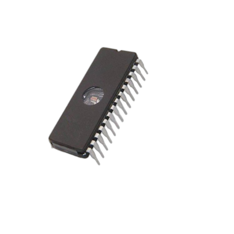

ADI 5962-9756401QXA(AD976SD)
- High-speed 16-bit SAR ADC with 100 kSPS throughput rate on single +5V supply
- Factory calibrated for offset, gain, linearity, SNR, and THD — no user trimming required
- ±10V analog input range — direct interface to standard industrial and military signal levels
- Internal 2.5V reference with external reference override capability
- On-chip clock, BUSY signal, and high-speed parallel interface — complete ADC solution
Single-supply operation in a 16-bit ADC was not always straightforward — most precision converters at this resolution required dual ±12V or ±15V supplies, adding power supply complexity and board area to military system designs. The ADI 5962-9756401QXA changes that. As the military SMD designation for Analog Devices' AD976SD processed to MIL-STD-883B, it delivers 16-bit resolution at 100 kSPS from a single +5V rail, with a ±10V analog input range handled internally through the BiCMOS architecture — no external input conditioning or supply conversion required.
The AD976 is factory calibrated at manufacture, with each device tested against offset, gain, linearity, SNR, and THD limits before shipment. That means the 5962-9756401QXA arrives as a fully characterized, production-verified ADC — not a device whose performance is inferred from a lot sample. The internal 2.5V reference can be overridden by an external reference for applications requiring tighter drift performance, and the on-chip clock and BUSY output complete the conversion timing interface without external components. For military procurement teams, the 5962-9756401QXA provides a standardized DoD acquisition path under SMD 5962-97564 with full MIL-STD-883B qualification documentation.
Related Products For Your Business
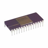
For defense procurement teams sourcing the ADI 5962-9756401QXA, the single-supply +5V operation is often the specification that makes the design decision straightforward. Military systems increasingly standardize on +5V and lower supply rails to reduce SWaP (Size, Weight, and Power) — and a 16-bit ADC that handles ±10V inputs from a single +5V supply without external level shifting or dual supplies eliminates a supply rail, reduces board space, and cuts the component count in the power distribution network. Processed to MIL-STD-883B under SMD 5962-97564 in a 28-lead ceramic DIP, the 5962-9756401QXA delivers that capability with full DoD qualification traceability.
5962-9756401QXA Architecture: Factory-Calibrated BiCMOS SAR for Military Signal Chains
The AD976 BiCMOS process combines bipolar precision with CMOS power efficiency — the architecture that allows it to achieve 89 dB typical SNR at 100 kSPS on a 100 mW budget from a single supply. Factory calibration addresses the limitation of uncalibrated SAR ADCs: each device is individually tested against INL, DNL, offset, gain, SNR, and THD limits, so the procurement specification and the delivered performance match without any user trimming or calibration step in the field. The internal 2.5V reference provides a convenient reference source for low-drift applications; for designs requiring tighter temperature coefficient performance, the reference pin accepts an external override from a precision military reference such as the 5962-9078501MLA AD780S, which provides 3 ppm/°C maximum drift in the same MIL-STD-883 qualification framework.
5962-9756401QXA vs AD976A Military Variant: Throughput Rate Selection
The AD976 family spans two throughput rates in the same architecture:
| 5962-9756401QXA (AD976S) | AD976A Military Variant | |
|---|---|---|
| Throughput Rate | 100 kSPS | 200 kSPS |
| Resolution | 16-bit | 16-bit |
| Supply | Single +5V | Single +5V |
| Input Range | ±10V | ±10V |
| Power | 100 mW max | 100 mW max |
| Best For | Standard military data acquisition | Higher-bandwidth signal chains |
For most military sensor digitization and data acquisition applications — inertial sensors, pressure transducers, resolver outputs from the 5962-9096201MQA AD2S80A RDC, strain gauges — the 100 kSPS rate of the 5962-9756401QXA is more than sufficient. The AD976A military variant doubles the throughput rate in the same package and power envelope for applications where signal bandwidth demands it.
Sourcing the ADI 5962-9756401QXA
The AD976SD in its military ceramic DIP package is an active-specification component in long-lifecycle defense and avionics programs where single-supply 16-bit ADC capability with MIL-STD-883B qualification is a hard requirement. We maintain verified inventory with full lot traceability, certificate of conformance, and anti-counterfeit inspection. Contact us today to confirm availability and request a quote — our team responds within 24 hours.
- Factory-calibrated to SNR and THD — no user calibration step required at board assembly or in the field
- Single +5V supply eliminates dual supply rail requirement — reduces SWaP in power-constrained military systems
- ±10V input range directly accepts standard industrial and military analog signal levels
- Byte mode enables connection to 8-bit processor buses without external demultiplexing logic
- BUSY output integrates cleanly with DMA or interrupt-driven data acquisition firmware architectures
- Compatible reference input accepts external precision military references for tighter drift applications
- Separate analog and digital supply pins allow independent analog/digital power plane routing
- Full lot traceability and MIL-STD-883B certificate of conformance on every order
Frequently Asked Questions (FAQ)
What Is the ADI 5962-9756401QXA and What Is Its Commercial Equivalent?
The 5962-9756401QXA is the military SMD procurement designation for Analog Devices’ AD976SD, processed to MIL-STD-883B under drawing 5962-97564. It is a 16-bit, 100 kSPS BiCMOS SAR ADC with single +5V supply operation, ±10V analog input range, factory calibration, internal 2.5V reference, on-chip clock, and a 16-bit parallel interface, in a 28-lead ceramic DIP package rated for military operation from –55°C to +125°C.
What Does Factory Calibration Mean for the AD976?
Factory calibration means every AD976 device is individually tested against offset error, full-scale gain error, INL, DNL, SNR, and THD limits before shipment — not just sampled from the lot. The device is adjusted during the manufacturing process to minimize linearity errors, so the production-tested specifications in the datasheet reflect what each individual device must meet, not population statistics.
Can the 5962-9756401QXA Accept an External Reference?
Yes. The internal 2.5V reference is available at the REF pin and can be overridden by an external precision reference. Connecting an external reference bypasses the internal reference and allows the use of lower-drift references such as the 5962-9078501MLA AD780S for applications where the internal reference’s temperature coefficient is insufficient for the system accuracy budget.
How Does the AD976 Interface to 8-Bit Processor Buses?
The AD976 includes a BYTE mode that splits the 16-bit conversion result into two sequential 8-bit bytes, accessible through the same 16 data lines. In byte mode, the first read returns the high byte (D15–D8) and the second returns the low byte (D7–D0). This eliminates the need for external demultiplexing logic when interfacing to 8-bit military processor buses.
How Do I Request a Quote for the ADI 5962-9756401QXA?
Submit an inquiry through our website contact form or email our sales team directly. We will respond within 24 hours with pricing, availability, and lead time — and can discuss long-term supply agreements for production programs.