ADI AD620ANZ
- Single external resistor sets gain from 1 to 10,000 — no internal resistor network matching required
- Low input offset voltage: 50 µV maximum with 0.6 µV/°C maximum drift (A grade)
- Low power operation: 1.3 mA maximum supply current from ±2.3V to ±18V supply range
- 100 dB minimum CMRR at G=10 with 9 nV/√Hz input voltage noise at 1 kHz
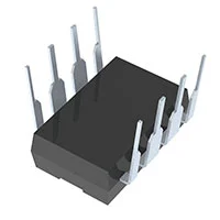
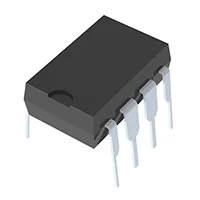
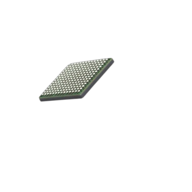
- 8-lead plastic DIP package — industry-standard footprint for direct board integration
The ADI AD620ANZ is the A-grade, 8-lead plastic DIP variant of Analog Devices' AD620 instrumentation amplifier — one of the most widely deployed in-amp architectures in precision signal chain design. A single external resistor connected between pins 1 and 8 sets the gain anywhere from 1 to 10,000, replacing the matched resistor networks and multi-component gain-setting arrangements that three op amp IA discrete designs require. The result is a complete instrumentation amplifier in an 8-lead package that is both smaller and more accurate than the discrete alternatives it replaces, at 1.3 mA maximum supply current that makes it practical for battery-powered and remote sensor applications.
The A-grade designation of the AD620ANZ specifies 50 µV maximum input offset voltage and 0.6 µV/°C maximum drift — tight enough for weigh scale interfaces, bridge sensor amplification, and precision transducer signal conditioning where the in-amp's offset contribution must stay small relative to the full-scale signal. Superbeta processing in the input stage holds input bias current to 1.0 nA maximum, which keeps the voltage error from source resistance small across a wide range of sensor impedances. The 100 dB minimum CMRR at G=10 rejects the common-mode interference that couples into sensor cables in industrial and field environments. For procurement teams sourcing the AD620ANZ, it is an active-production component with broad distributor availability and a well-established design-in history across industrial, medical, and instrumentation markets.

Related Products For Your Business
For procurement teams sourcing the AD620ANZ, the practical appeal of this component is the combination of well-understood performance, broad availability, and a design-in base that spans decades of instrumentation and sensor interface applications. The single-resistor gain setting — the feature that distinguished the original AD620 from three op amp discrete alternatives — remains the reason engineers specify it: one component, one resistor, a complete instrumentation amplifier that outperforms the discrete equivalent in offset, noise, CMRR, and board area simultaneously. As the A-grade variant in an 8-lead plastic DIP, the AD620ANZ is the standard stocking unit for industrial and instrumentation design work across the –40°C to +85°C operating range.
AD620ANZ Architecture: Superbeta Input Stage and Single-Resistor Gain
The AD620’s three op amp topology uses a matched pair of Superbeta NPN input transistors in the input stage — the technology that achieves 1.0 nA maximum input bias current without the noise penalty that FET input stages impose at low frequencies. Gain is set by a single resistor between the RG pins: the formula G = (49.4 kΩ / RG) + 1 covers the full 1 to 10,000 range with standard resistor values. Because the gain-setting resistor connects directly between the two internal feedback nodes of the input stage, there is no external op amp feedback path to mismatch — gain accuracy and gain TC depend on the tolerance and TC of a single external resistor, which is a much simpler error budget than the matched resistor networks required in discrete designs. The output stage REF pin allows the AD620ANZ output to be offset to any voltage within the output swing range, enabling direct interface to single-supply ADCs without an external level-shifting stage.
AD620ANZ vs AD620BNZ: A Grade vs B Grade Selection
The AD620 family offers two accuracy grades in the plastic DIP package. The selection is straightforward:
| AD620ANZ | AD620BNZ | |
|---|---|---|
| Input Offset Voltage | 50 µV Maximum | 25 µV Maximum |
| Input Offset Drift | 0.6 µV/°C Maximum | 0.3 µV/°C Maximum |
| Gain Nonlinearity | 40 ppm Maximum | 10 ppm Maximum |
| Package | 8-Lead PDIP | 8-Lead PDIP |
| Temperature Range | –40°C to +85°C | –40°C to +85°C |
| Best For | General instrumentation, cost-sensitive designs | Highest precision, low-gain accuracy-critical designs |
For the majority of bridge sensor, strain gauge, and transducer interface applications where the signal conditioning chain tolerates 50 µV of in-amp offset, the AD620ANZ is the correct choice. For designs where the in-amp operates at low gain and the offset budget is tight — precision weigh scales, high-resolution data acquisition — the AD620BNZ’s tighter specifications justify the premium. For military programs requiring the –55°C to +125°C temperature range and ceramic packaging, the AD620SQ/883B is the qualified military variant.
Sourcing the ADI AD620ANZ
The AD620ANZ is an active-production standard product with broad distribution availability. We carry verified inventory with full lot traceability and can support both prototype quantities and production volume orders. Our team responds to inquiries within 24 hours with pricing, availability, and lead time. Contact us today to request a quote for the ADI AD620ANZ.
- Single external resistor sets gain 1 to 10,000 — no matched resistor networks, no gain trim required
- REF pin enables direct single-supply ADC interface without external level-shifting components
- Superbeta input stage achieves 1.0 nA maximum bias current — low error across wide sensor impedance range
- Output short-circuit protected — fault-tolerant in industrial field environments
- Pin-compatible with AD621, AD622, AD623 on standard EVAL-INAMP-62RZ evaluation board
- Available in SOIC (AD620ARZ) for surface-mount designs with identical electrical specifications
- Military grade AD620SQ/883B available for programs requiring –55°C to +125°C ceramic packaging
- Full lot traceability and certificate of conformance available on request
Frequently Asked Questions (FAQ)
What Is the ADI AD620ANZ and How Does It Differ From the AD620BNZ?
The AD620ANZ is the A-grade, 8-lead plastic DIP variant of the AD620 instrumentation amplifier, with 50 µV maximum input offset voltage and 0.6 µV/°C maximum drift, rated for –40°C to +85°C industrial operation. The AD620BNZ is the B-grade variant with tighter specifications — 25 µV maximum offset and 0.3 µV/°C maximum drift — for designs with more demanding accuracy requirements. Both use the same single-resistor gain-setting architecture and 8-lead PDIP package.
How Is Gain Set on the AD620ANZ?
Gain is set by a single external resistor connected between pins 1 and 8 (the RG pins), using the formula G = (49.4 kΩ / RG) + 1. For example, a 49.9Ω resistor sets G=1000, and leaving the pins open sets G=1. Standard 1% resistor values cover the full gain range from 1 to 10,000 without any additional components or adjustments.
Is the AD620ANZ Pin-Compatible With Other ADI Instrumentation Amplifiers?
The AD620ANZ shares the standard 8-lead in-amp pinout with the AD621, AD622, and AD623, and is compatible with the EVAL-INAMP-62RZ evaluation board. The AD620SQ/883B military variant in ceramic DIP uses the same pinout, enabling direct substitution for programs transitioning between industrial and military qualification levels.
What Is the Military Grade Equivalent of the AD620ANZ?
The military grade equivalent is the AD620SQ/883B — the same AD620 die in an 8-lead ceramic DIP (CERDIP) package, processed to MIL-STD-883B, rated for –55°C to +125°C operation. For programs requiring the extended temperature range and hermetic packaging of a military-qualified component, the AD620SQ/883B is the direct upgrade path from the AD620ANZ.
How Do I Request a Quote for the ADI AD620ANZ?
Submit an inquiry through our website contact form or email our sales team directly. We will respond within 24 hours with pricing, availability, and lead time — and can discuss volume pricing or long-term supply agreements if needed.