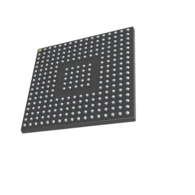
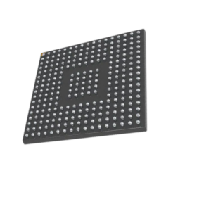
ADI AD9613BCPZ-250
- Dual 12-bit ADCs at 250 MSPS with 69.6 dBFS SNR and 86 dBc SFDR for high dynamic range radar signal digitization
- 400 MHz full-power bandwidth and IF sampling up to 400 MHz supporting direct IF sampling of wideband radar and EW signals
- Flexible LVDS output formatting (interleaved or channel multiplexed) with integer 1-to-8 clock divider for system integration
- Single 1.8 V supply operation with integrated reference and duty cycle stabilizer simplifying avionics power distribution
- SYNC input for multi-device synchronization and 95 dB channel isolation for phased array radar applications
Related Products For Your Business
The AD9613BCPZ-250 provides dual 12-bit ADC performance at 250 MSPS per channel, making it ideal for aerospace and defense applications requiring high-speed dual-channel digitization with excellent dynamic range. You get 69.6 dBFS SNR and 86 dBc SFDR at 185 MHz input frequency with a 400 MHz full-power bandwidth that enables direct IF sampling of wideband radar and electronic warfare signals up to 400 MHz. The dual ADC architecture supports simultaneous sampling of two input channels, critical for I/Q demodulation systems in phased array radar where phase-coherent signal processing is essential for beamforming and direction finding. The single 1.8 V supply operation for both analog and digital sections reduces power distribution complexity compared to 3.3 V ADCs, while LVDS outputs provide excellent noise immunity and reduced power consumption for high-speed signal paths through avionics backplanes. The SYNC input enables synchronization of multiple AD9613 devices for phased array radar systems requiring dozens or hundreds of coherent channels, while the 95 dB channel isolation ensures minimal crosstalk between adjacent channels in tightly packed receiver modules. With flexible LVDS output formatting (interleaved or channel multiplexed), integer 1-to-8 clock divider, and integrated reference with duty cycle stabilizer, the AD9613BCPZ-250 provides comprehensive system integration features that simplify design of advanced radar and EW digitization systems.
Ultra-High-Speed Dual 12-Bit Pipeline ADC Architecture for Phased Array Radar Systems
The dual 12-bit ADC cores digitize at 250 MSPS through a monolithic sampling architecture with integrated sample-and-hold and voltage reference on the same silicon die. The 400 MHz full-power bandwidth represents a significant advancement over previous generations of 12-bit ADCs, enabling direct IF sampling of wideband radar returns and electronic warfare signals up to 400 MHz without the need for intermediate frequency conversion stages. This capability reduces system complexity, component count, and potential signal degradation associated with multi-stage downconversion architectures in phased array radar systems where receiver modules are distributed across large antenna apertures. Differential analog inputs with programmable voltage range (1.4 V p-p to 2.0 V p-p) provide excellent immunity to common-mode noise and ground loops while offering flexibility to optimize dynamic range for different signal levels encountered in radar and EW applications. The proprietary differential input architecture maintains excellent SNR performance for input frequencies up to 400 MHz, which is critical for preserving signal fidelity in wideband electronic warfare receivers that must capture weak signals in the presence of strong interference.
The AD9613 architecture provides excellent linearity characteristics with differential nonlinearity (DNL) of ±0.5 LSB and integral nonlinearity (INL) of ±0.8 LSB typical. This linearity ensures consistent conversion accuracy across the entire input range, critical for radar systems where precise amplitude measurement determines target detection thresholds and range accuracy. The effective number of bits (ENOB) of 11.1 at 185 MHz input frequency provides usable resolution close to the theoretical 12-bit limit at ultra-high input frequencies, enabling detailed signal characterization in electronic warfare applications where subtle signal variations indicate sophisticated modulation schemes or low-probability-of-intercept signals. The 86 dBc SFDR at 185 MHz ensures that spurious tones remain well below the radar system’s dynamic range requirements, preventing false target detection or signal degradation in sensitive EW receivers operating in congested electromagnetic environments. The 95 dB channel isolation and crosstalk specification is particularly important for phased array radar systems where multiple AD9613 devices are densely packed in receiver modules, ensuring minimal interference between adjacent channels that could degrade beamforming accuracy.
Integrated Reference and Advanced System Integration Features for Avionics Applications
The integrated voltage reference represents a significant architectural advancement over traditional high-speed ADC designs, eliminating the need for external reference components while maintaining excellent accuracy across temperature variations. The internal reference provides a stable 1.75 V full-scale input range with typical reference voltage accuracy of ±10 mV offset error and ±4% gain error, which is sufficient for most aerospace applications requiring high dynamic range but not requiring calibration-grade precision. This integration eliminates the need for external voltage reference ICs, associated filtering capacitors, and PCB routing complexity, reducing component count, board space requirements, and potential failure points in mission-critical avionics systems. The duty cycle stabilizer (DCS) compensates for variations in the ADC clock duty cycle, which is critical for maintaining performance in systems where clock jitter and duty cycle variations can degrade SNR and SFDR at ultra-high sampling rates. The DCS ensures consistent performance across the industrial temperature range without requiring precise clock source conditioning, simplifying clock distribution network design in phased array radar systems where clock signals are distributed to dozens or hundreds of receiver modules.
Beyond the reference and DCS, the AD9613 incorporates flexible power management features that optimize system-level power consumption in radar and EW applications. Flexible power-down options allow significant power savings when ADC channels are not actively digitizing, which is critical for multi-mode radar systems that switch between different operational modes based on threat scenarios. Standby power consumption of 90 mW and power-down power consumption of 10 mW represent substantial reductions compared to the 770 mW typical operating power consumption, enabling duty-cycled operation in energy-constrained platforms such as unmanned aerial vehicles (UAVs) and portable tactical systems. The integer 1-to-8 input clock divider (625 MHz maximum input) enables flexible clock architecture design while maintaining low jitter performance through the on-chip duty cycle stabilizer, allowing system designers to optimize clock distribution networks based on available clock sources and jitter performance requirements. Fast overrange and threshold detect features provide early warning of signal clipping or threshold crossing events, enabling automatic gain control (AGC) systems to respond rapidly to changing signal environments in dynamic EW scenarios.
LVDS Digital Interface and Multi-Device Synchronization for Phased Array Radar
The AD9613 provides 12-bit data from each of the dual ADC cores through two external LVDS (ANSI-644 compatible) output ports, offering excellent noise immunity and reduced power consumption compared to CMOS outputs. LVDS technology is particularly advantageous for avionics systems where high-speed data paths run through long traces in backplanes between multiple processing boards, as the differential signaling provides excellent immunity to common-mode noise and ground potential differences that inevitably exist in complex avionics chassis with distributed power and ground references. The LVDS output data can be formatted either as interleaved (where both channels’ data are time-multiplexed on a single port) or channel multiplexed (where each channel’s data is output on a separate port), providing system designers with flexibility to optimize interface timing and FPGA resource utilization based on specific application requirements. The SYNC input enables synchronization of multiple AD9613 devices for phased array radar systems requiring dozens or hundreds of coherent channels, which is essential for maintaining phase coherence across the entire antenna aperture for accurate beamforming and direction finding.
A dedicated data clock output (DCO±) provides precise timing for FPGA capture logic, while programmable clock and data alignment features enable optimization of timing relationships for different FPGA architectures and interface requirements. The serial port interface (SPI-compatible) provides comprehensive control over ADC configuration and operation, including data format selection (twos complement or offset binary), power-down mode activation, gain adjustment, and test pattern generation. This SPI control capability eliminates the need for hardware configuration pins that would increase package size and routing complexity, enabling the 64-lead LFCSP package despite the rich feature set. The 3-pin, 1.8 V SPI port supports register programming and register readback, enabling system monitoring and diagnostic capabilities that are critical for mission-critical aerospace applications where health monitoring and fault detection are essential for system reliability. Pin compatibility with the AD9643 (14-bit dual ADC), AD6649, and AD6643 provides a migration path for system upgrades without requiring complete PCB redesign, which is valuable for aerospace programs with long lifecycles and evolutionary upgrade requirements.
AD9613BCPZ-250 vs AD9643BCPZ-250: Dual ADC Resolution Comparison
Dual ADC options from Analog Devices represent different resolution grades optimized for different performance requirements in aerospace radar and electronic warfare systems. The comparison table below shows the key differences between the 12-bit AD9613 and the 14-bit AD9643, both operating at 250 MSPS in the same 64-lead LFCSP package.
表格
| Parameter | AD9613BCPZ-250 (12-Bit Industrial) | AD9643BCPZ-250 (14-Bit Industrial) |
|---|---|---|
| Generation | Cost-Optimized High Performance | High-Resolution Flagship |
| Resolution | 12 bits | 14 bits |
| Channels | 2 (Dual) | 2 (Dual) |
| Sampling Rate | 250 MSPS per channel | 250 MSPS per channel |
| SNR (at 185 MHz) | 69.6 dBFS (typical) | 70.5 dBFS (typical) |
| SFDR (at 185 MHz) | 86 dBc (typical) | 85 dBc (typical) |
| ENOB | 11.1 bits (at 185 MHz) | 11.4 bits (at 185 MHz) |
| Full-Power Bandwidth | 400 MHz | 400 MHz |
| IF Sampling | Up to 400 MHz | Up to 400 MHz |
| DNL | ±0.5 LSB (typical) | ±0.4 LSB (typical) |
| INL | ±0.8 LSB (typical) | ±1.0 LSB (typical) |
| Power Consumption | 770 mW at 250 MSPS | 790 mW at 250 MSPS |
| Supply Voltage | +1.8 V (single supply) | +1.8 V (single supply) |
| Output Interface | LVDS (interleaved or channel multiplexed) | LVDS (interleaved or channel multiplexed) |
| Package | 64-Lead LFCSP (9mm x 9mm, EP) | 64-Lead LFCSP (9mm x 9mm, EP) |
| Pin Compatibility | Pin-compatible with AD9643 | Pin-compatible with AD9613, AD6649, AD6643 |
| Operating Temperature | −40°C to +85°C (Industrial) | −40°C to +85°C (Industrial) |
| Integer Clock Divider | 1-to-8 (625 MHz maximum) | 1-to-8 (625 MHz maximum) |
| SYNC Input | Yes, for multi-device synchronization | Yes, for multi-device synchronization |
| Best Application Fit | Cost-Optimized Dual-Channel Radar & EW | High-Resolution Dual-Channel Radar & EW |
If your application requires maximum resolution with minimal system redesign, the AD9643 provides 14-bit performance in the same footprint as the AD9613, with only 20 mW additional power consumption at 250 MSPS. The pin compatibility between AD9613 and AD9643 allows direct substitution on the same PCB layout without requiring routing changes, enabling product differentiation or performance upgrades during the product lifecycle. For applications where the AD9613’s 12-bit resolution provides adequate performance, the cost-optimized architecture provides approximately 2.5% power savings (770 mW vs. 790 mW) while maintaining similar dynamic range characteristics. The 400 MHz full-power bandwidth and IF sampling capability up to 400 MHz are identical between both devices, ensuring equivalent signal capture capability for wideband radar and EW applications. The dual-channel architecture and multi-device synchronization via SYNC input are identical, making both devices equally suitable for phased array radar systems requiring coherent multi-channel digitization across large antenna apertures.
Sourcing ADI AD9613BCPZ-250 with Industrial Grade Validation
The BCPZ-250 tray packaging works well for prototype and qualification builds of the AD9613 in the 64-lead LFCSP package with exposed thermal pad, which provides enhanced thermal dissipation compared to standard LFCSP packages without exposed pads. The exposed thermal pad requires proper thermal vias and soldering to ground plane on the PCB for optimal thermal performance, which is critical for maintaining specifications in high-power applications running at 250 MSPS dual-channel operation. The 9mm x 9mm package footprint provides approximately 59% board space reduction compared to 100-lead TQFP packages (14mm x 14mm), enabling more compact avionics module designs and potentially reducing overall system weight—a critical consideration for aerospace applications where every gram impacts fuel consumption and payload capacity. We stock verified inventory with full lot traceability from the manufacturer to your facility, including documentation packages like Certificates of Conformity and material declarations that aerospace and defense contractors typically need for qualification processes. Anti-counterfeit inspection happens on every order to confirm authenticity, and we handle export compliance documentation for international shipments to defense contractors and aerospace manufacturers worldwide.
- Dual 12-bit architecture with 250 MSPS sampling rate per channel for high-speed dual-channel radar digitization
- 69.6 dBFS SNR and 86 dBc SFDR at 185 MHz for superior dynamic range at ultra-high frequencies
- 400 MHz full-power bandwidth supporting direct IF sampling up to 400 MHz in avionics applications
- Excellent linearity with DNL = ±0.5 LSB and INL = ±0.8 LSB
- Flexible LVDS output formatting (interleaved or channel multiplexed) for system integration
- Single 1.8 V supply operation reducing power distribution complexity
- Integrated reference and duty cycle stabilizer enhancing performance across industrial temperature range
- SYNC input for multi-device synchronization in phased array radar systems
- 95 dB channel isolation minimizing crosstalk in densely packed receiver modules
- Industrial temperature range (−40°C to +85°C) in compact 64-lead LFCSP package
- Integer 1-to-8 clock divider (625 MHz maximum input) enabling flexible clock architecture
- Pin-compatible with AD9643 for 14-bit upgrade path without PCB redesign
Frequently Asked Questions (FAQ)
What Is the Difference Between AD9613BCPZ-250 and AD9643BCPZ-250?
These two devices represent different resolution grades of dual ADC technology with identical pinout and package, enabling direct substitution without PCB redesign. The AD9613 is a cost-optimized 12-bit dual ADC, while the AD9643 is a high-resolution 14-bit dual ADC, both operating at 250 MSPS in the same 64-lead LFCSP package. For applications requiring maximum resolution, the AD9643 provides 14-bit performance with 70.5 dBFS SNR and 85 dBc SFDR at 185 MHz, compared to the AD9613’s 69.6 dBFS SNR and 86 dBc SFDR at the same input frequency. The pin compatibility allows direct substitution on the same PCB layout, enabling product differentiation or performance upgrades during the product lifecycle without requiring routing changes or new PCB designs. Power consumption differs slightly between the two devices, with the AD9613 consuming 770 mW typical at 250 MSPS compared to the AD9643’s 790 mW at the same sampling rate, representing approximately 2.5% power savings for the 12-bit version. For applications where the AD9613’s 12-bit resolution provides adequate performance for radar and EW requirements, the cost-optimized architecture provides value while maintaining similar dynamic range characteristics and system-level features.
What Is the Power Consumption of AD9613BCPZ-250 at 250 MSPS?
The device consumes 770 mW typical at 250 MSPS in LVDS mode with the 1.8 V analog and digital supplies at nominal voltages, operating dual ADC cores simultaneously. This power consumption breaks down to approximately 252 mA to 275 mA from the AVDD supply (1.8 V analog) and 176 mA to 210 mA from the DRVDD supply (1.8 V digital output drivers), totaling 428 mA to 485 mA of current draw at typical operating conditions. The 770 mW typical power consumption represents the power draw when both ADC cores are actively digitizing at maximum sampling rate, which is relevant for continuous wave radar systems or wideband EW receivers that require uninterrupted signal capture. For applications that do not require continuous operation, flexible power-down options enable significant power savings. Standby power consumption is 90 mW, and full power-down mode reduces power consumption to just 10 mW, enabling duty-cycled operation in energy-constrained platforms such as unmanned aerial vehicles (UAVs) and portable tactical systems. The single 1.8 V supply operation for both analog and digital sections reduces power distribution complexity and eliminates the need for separate voltage regulators for analog and digital domains.
Does AD9613BCPZ-250 Support On-Chip Reference Voltage?
Yes, this device features an internal ADC voltage reference that eliminates the need for external reference components in most applications. The internal reference provides a stable 1.75 V full-scale input range with typical reference voltage accuracy of ±10 mV offset error and ±4% gain error, which is sufficient for most aerospace applications requiring high dynamic range but not requiring calibration-grade precision. This integration eliminates the need for external voltage reference ICs, associated filtering capacitors, and PCB routing complexity, reducing component count, board space requirements, and potential failure points in mission-critical avionics systems. The integrated reference accuracy meets the requirements of most radar and EW applications where signal processing gain variations can be calibrated out digitally. For applications requiring calibration-grade precision or specific reference voltage values, external reference mode can be implemented, though this is not typically required for the AD9613’s intended aerospace and defense applications. The reference voltage stability across the industrial temperature range of −40°C to +85°C is ensured by internal temperature compensation circuitry, maintaining consistent performance in harsh avionics environments where temperature variations can be extreme.
How Do I Synchronize Multiple AD9613BCPZ-250 Devices for Phased Array Radar Systems?
The AD9613 includes a SYNC input that enables synchronization of multiple devices for phased array radar systems requiring dozens or hundreds of coherent channels. The SYNC input is CMOS/LVDS compatible with internal bias at 0.9 V and an input voltage range from AGND to AVDD, accepting both CMOS and LVDS level signals for maximum flexibility in clock distribution network design. Synchronization is achieved by simultaneously asserting the SYNC input on all AD9613 devices in the array, which resets internal timing circuits and aligns the sampling phase of all ADCs to the same edge of the distributed clock. This synchronization capability is essential for maintaining phase coherence across the entire antenna aperture for accurate beamforming and direction finding in phased array radar systems. The combined use of SYNC input and integer 1-to-8 clock divider enables flexible clock distribution architectures while maintaining phase coherence across large antenna arrays with hundreds of receiver modules. System designers should ensure careful clock distribution network design to minimize skew between different AD9613 devices, as clock skew directly translates to phase errors that degrade beamforming accuracy. The 95 dB channel isolation specification ensures minimal crosstalk between adjacent channels in densely packed receiver modules, which is particularly important when multiple AD9613 devices are closely spaced on the same PCB or module.
Can AD9613BCPZ-250 Be Controlled via SPI Serial Port?
Yes, this ADC features a comprehensive SPI-compatible serial port interface that provides complete control over device configuration and operation. The SPI interface consists of three pins: SCLK (serial clock), SDIO (serial data input/output), and CSB (chip select, active low). The serial port operates from a 1.8 V supply and supports register programming and register readback, enabling system monitoring and diagnostic capabilities that are critical for mission-critical aerospace applications where health monitoring and fault detection are essential for system reliability. Through this serial interface, users can configure data format (twos complement or offset binary), activate power-down mode for reduced power consumption during idle periods, adjust gain for optimizing input dynamic range, and generate test patterns for system-level testing and calibration. This comprehensive SPI control capability eliminates the need for hardware configuration pins that would increase package size and routing complexity, enabling the compact 64-lead LFCSP package despite the rich feature set. The SPI interface also allows dynamic reconfiguration of ADC parameters during operation, enabling adaptive radar and electronic warfare systems that can optimize performance based on real-time threat or environmental conditions. Register readback capability enables system health monitoring, fault detection, and diagnostic functions that are essential for mission-critical aerospace applications where system reliability and maintainability are paramount requirements.
How Do I Request a Quote for ADI AD9613BCPZ-250?
Submit an inquiry through our website contact form or email our sales team directly. We will respond within 24 hours with pricing, availability, and lead time, and can discuss long-term supply agreements for radar and EW production programs requiring industrial-grade dual ADC components with full lot traceability and anti-counterfeit inspection.