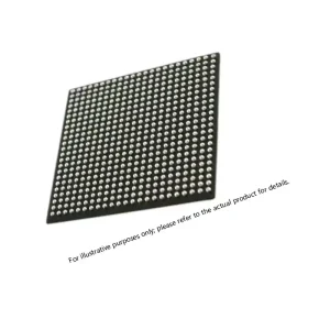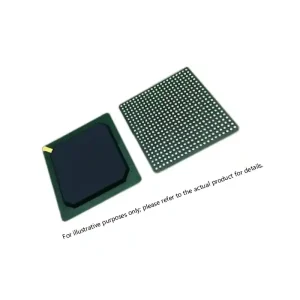
XILINX XCKU085-2FLVB1760E
- Number of Inputs: 676
- Supply Voltage-Nom: 0.95
- Supply Voltage-Min: 0.922
- Supply Voltage-Max: 0.979
- Min Operating Temperature: 0
- Max Operating Temperature: 100
- Temperature Grade: OTHER
- Number of Terminals: 1760
- JEDEC Package Code: S-PBGA-B1760
XILINX XCKU085-2FLVB1760E is a programmable logic device. Review the exact-part parameters, package and temperature requirements before approving a source or alternate.
Related Products For Your Business
XCKU085-2FLVB1760E Technical Overview: Verified Parameters Before Sourcing
XILINX XCKU085-2FLVB1760E is a programmable logic device cataloged in FPGA & CPLD for Aerospace & Defense, Avionics Systems, Radar & Electronic Warfare, Satellite & Space programs. Unlike a family-level listing, the complete ordering code matters: package, temperature grade, speed option, screening level and shipment format can change with a suffix. The structured reference data for this exact part identifies Number of Inputs 676, Supply Voltage-Nom 0.95, Supply Voltage-Min 0.922, Supply Voltage-Max 0.979.
These values are useful for initial BOM and sourcing review, but engineering approval should still use the latest manufacturer-controlled datasheet, package drawing and change notices. For availability, lot/date code and documentation, send Sparkle Electronics the complete XCKU085-2FLVB1760E requirement.
XCKU085-2FLVB1760E Key Specifications
| Parameter | XCKU085-2FLVB1760E |
|---|---|
| Number of Inputs | 676 |
| Supply Voltage-Nom | 0.95 |
| Supply Voltage-Min | 0.922 |
| Supply Voltage-Max | 0.979 |
| Min Operating Temperature | 0 |
| Max Operating Temperature | 100 |
| Temperature Grade | OTHER |
| Number of Terminals | 1760 |
| JEDEC Package Code | S-PBGA-B1760 |
What the Specifications Mean in a Design Review
For this programmable logic device, the main compatibility checks are logic density, I/O count, speed grade, configuration flow, package escape routing, power rails and toolchain support. A replacement should not be approved from the family name alone. The values below need to be checked against the schematic, PCB footprint, power tree, timing constraints, thermal analysis and program qualification baseline:
- Number of Inputs: 676
- Supply Voltage-Nom: 0.95
- Supply Voltage-Min: 0.922
- Supply Voltage-Max: 0.979
- Min Operating Temperature: 0
- Max Operating Temperature: 100
- Temperature Grade: OTHER
Minimum and maximum values are not interchangeable with typical test values, and package-level compatibility does not guarantee pin, timing or firmware compatibility. Where the assembly is used in high-reliability equipment, confirm the required screening, traceability, lead finish and environmental documentation before purchase.
XCKU085-2FLVB1760E and Related XILINX Devices
The following pages provide useful internal comparison points. They are related sourcing options, not automatically drop-in replacements:
- XILINX XC2V2000-5FG676I — compare the exact architecture, package, speed or grade before substitution.
- XILINX XC3S700AN-4FGG484I — compare the exact architecture, package, speed or grade before substitution.
- XILINX XC5VFX130T-1FFG1738I — compare the exact architecture, package, speed or grade before substitution.
- XILINX XC5VSX240T-1FFG1738I — compare the exact architecture, package, speed or grade before substitution.
When comparing these devices, start with the exact function and architecture, then verify package and pinout, voltage rails, speed or bandwidth, operating temperature and qualification grade. If any of those differ, an engineering redesign or requalification may be required.
Package, Temperature and Ordering-Code Checks
The orderable code XCKU085-2FLVB1760E must be kept intact on the RFQ. Confirm the manufacturer marking, package drawing, terminal finish, moisture handling, operating-temperature requirement and packing format. For obsolete or long-stored material, define acceptable date codes and inspection criteria before quotation rather than after delivery.
Sourcing teams should also request the documentation appropriate to the program: Certificate of Conformance, packing and label photographs, lot/date-code information, traceability, visual inspection, X-ray or electrical testing when required. See our quality-control approach and the broader FPGA & CPLD selection.
Applications and Procurement Context
XCKU085-2FLVB1760E may be evaluated for Aerospace & Defense, Avionics Systems, Radar & Electronic Warfare, Satellite & Space systems where its verified electrical limits, package and temperature range match the approved design. Typical work includes new production, repair, lifecycle extension and last-time-buy planning. Application labels describe catalog relevance; final suitability remains a system-level engineering decision.
Frequently Asked Questions
What are the main XCKU085-2FLVB1760E parameters?
The key reference values are Number of Inputs 676, Supply Voltage-Nom 0.95, Supply Voltage-Min 0.922, Supply Voltage-Max 0.979. The complete table above should be reviewed together with the current manufacturer documentation and the operating conditions stated in that document.
Can another XILINX part replace XCKU085-2FLVB1760E?
Not from the model name alone. Compare function, architecture, pinout, package, voltage, speed, temperature and qualification grade. The linked related devices are comparison starting points only.
What should be included in an RFQ?
Provide the exact part number, quantity, target delivery date, destination, acceptable date-code range and all documentation, screening or testing requirements. Submit the RFQ here.
Where can I review related components?
Browse FPGA & CPLD and the relevant Aerospace & Defense, Avionics Systems, Radar & Electronic Warfare, Satellite & Space landing pages for other product families and sourcing guidance.
Need XCKU085-2FLVB1760E pricing, availability or traceability details? Contact Sparkle Electronics with the exact order code and procurement requirements.