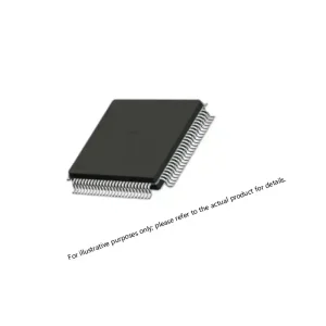
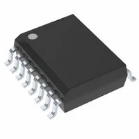
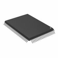
CYPRESS CY7C1371D-100AXI
- 18Mbit (512K × 36 / 1M × 18) NoBL™ flow-through synchronous SRAM — single-cycle read latency
- 100MHz clock, 8.5ns access time, zero dead cycles between back-to-back read/write operations
- Flow-through architecture delivers minimum read latency vs. pipelined NoBL™ — first data valid in one clock cycle
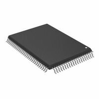
- 100-pin TQFP, industrial temperature −40°C to +85°C, 3.3V supply (3.0V to 3.6V)
- Obsolete lifecycle — verified lot stock available at Sparkle Electronics; immediate RFQ response
Cypress Semiconductor (now Infineon Technologies) offered the NoBL™ SRAM family in two architectural variants — pipelined and flow-through — to address two distinct system design priorities within the same NoBL™ no-dead-cycle framework. The CY7C1371D is the flow-through variant: where the pipelined CY7C1370D registers read data through an additional pipeline stage to achieve 167MHz operation at the cost of a two-cycle read latency, the flow-through CY7C1371D delivers read data in a single clock cycle, minimizing the latency between address presentation and data availability at the cost of a lower maximum clock frequency of 100MHz. The CY7C1371D-100AXI is available from stock at Sparkle Electronics, a specialized distributor serving defense electronics procurement teams, embedded systems engineers, and networking OEMs requiring verified sourcing of hard-to-find and obsolete SRAM with full lot traceability documentation and same-day RFQ response.
The CY7C1371D-100AXI carries an obsolete lifecycle designation — Infineon has discontinued manufacturing, and global supply consists exclusively of remaining distributor inventory. The AXI ordering suffix designates the 100-pin TQFP package with industrial temperature grade (−40°C to +85°C) in tube packaging. For programs in active production or sustaining operations that cannot be redesigned to accommodate a replacement memory architecture, securing verified lot stock from a traceable source is the only viable supply continuity path. Procurement engineers sourcing this part for aerospace and defense embedded computing, radar and electronic warfare signal processing, or networking equipment programs must act within a contracting window that closes as available inventory is depleted. Contact Sparkle Electronics immediately to confirm current stock levels and pricing.
Related Products For Your Business
Flow-Through vs. Pipelined NoBL™: A Procurement and Design Decision with No Equivalent Replacement
The architectural distinction between the CY7C1371D (flow-through) and CYPRESS CY7C1370D-167AXI (pipelined) is not a performance ranking — it is a latency vs. throughput trade-off that determined which device was specified at design time, and which now defines the only acceptable replacement in an obsolete supply environment. Systems that were designed to the CY7C1371D’s one-cycle read latency and the interface timing it implies cannot directly substitute the two-cycle pipelined CY7C1370D without firmware and possibly hardware modifications. This interface dependency makes obsolete NoBL™ flow-through SRAM one of the most procurement-critical memory categories in defense and networking sustainment programs. Engineers and procurement specialists searching for CY7C1371D-100AXI in stock, Cypress NoBL flow-through SRAM 18Mbit 100MHz, CY7C1371D-100AXI obsolete stock distributor, or CY7C1371D-100AXI last-time buy will find Sparkle Electronics maintains verified inventory with confirmed lot traceability. Submit an inquiry immediately to confirm current quantity and initiate procurement before stock is exhausted.
CY7C1371D-100AXI vs. CY7C1370D-167AXI: Choosing Between Flow-Through and Pipelined NoBL™
| Parameter | CY7C1371D-100AXI | CY7C1370D-167AXI |
|---|---|---|
| Availability | In Stock at Sparkle | In Stock at Sparkle |
| Lifecycle | Obsolete | Obsolete |
| NoBL™ Architecture | Flow-Through | Pipelined |
| Read Latency | 1 clock cycle | 2 clock cycles |
| Clock Frequency | 100MHz | 167MHz |
| Access Time | 8.5ns | 3.4ns |
| Effective Bandwidth | Lower (100MHz × 36-bit) | Higher (167MHz × 36-bit) |
| Capacity | 18Mbit (512K × 36 / 1M × 18) | 18Mbit (512K × 36 / 1M × 18) |
| Supply Voltage | 3.3V | 3.3V |
| Package | 100-pin TQFP | 100-pin TQFP |
| Temperature | −40°C to +85°C | −40°C to +85°C |
| Pin Compatible | No (different timing requirements) | No |
| JTAG (TQFP) | Not available | Not available |
The flow-through architecture is the correct original specification for system designs where controller firmware was written to receive read data one clock cycle after address presentation. Substituting the pipelined variant — even if physically installable — requires firmware timing modification to account for the additional pipeline stage and will produce incorrect behavior if applied without verification. Both variants are obsolete and require verified lot sourcing from a traceable distributor.
NoBL™ Flow-Through Operation: What Single-Cycle Latency Means in Practice
In a flow-through synchronous SRAM, the internal read path does not register data through an additional pipeline latch before presenting it to the output. The address is sampled at clock rising edge, the memory array is accessed, and valid data appears at the output pins within the same clock cycle — 8.5ns access time from address setup. For controllers that issue a read command and expect data in the immediately following clock cycle, this behavior is the minimum possible latency for a synchronous SRAM architecture and requires no pipeline-aware timing offset in firmware.
This single-cycle latency characteristic was the design-time rationale for specifying the CY7C1371D over the pipelined CY7C1370D in applications where memory access latency directly affected system response time — real-time radar tracking loops, electronic warfare response systems, and packet processing engines where the latency between address and data determines the system’s ability to meet its deterministic timing budget. For broader memory and storage requirements, Sparkle Electronics maintains inventory across active and obsolete SRAM categories including the dual-port CYPRESS CY7C0851AV-133BBI for programs where new design flexibility allows active lifecycle specifications.
Frequently Asked Questions
What does CY7C1371D-100AXI decode to?
CY7C = Cypress SRAM product family prefix; 1371 = NoBL™ flow-through synchronous SRAM, 18Mbit density; D = D-generation silicon revision; -100 = 100MHz clock frequency rating; A = TQFP package type; X = RoHS/lead-free compliant; I = industrial temperature grade (−40°C to +85°C); tube packaging. The 1370D is the pipelined counterpart at 167MHz; the 1371D is the flow-through counterpart at 100MHz.
Where can I buy CY7C1371D-100AXI in stock?
Sparkle Electronics maintains verified stock of the CY7C1371D-100AXI. Given the obsolete lifecycle and finite remaining global supply, procurement teams with ongoing production or sustainment requirements should submit an RFQ without delay to confirm current quantity and pricing. Contact our team — same-day response on pricing, lot documentation scope, and confirmed available quantity.
Can CY7C1371D-100AXI be substituted with CY7C1370D-167AXI?
Not directly. The pipelined CY7C1370D requires firmware to account for a two-cycle read latency, while the flow-through CY7C1371D delivers data in one cycle. Substituting the pipelined variant in a system designed for flow-through operation will produce incorrect read data timing unless the controller firmware is updated to compensate. Physical pin compatibility in the same 100-pin TQFP package must also be verified against the specific board layout. Substitution requires engineering review of both hardware timing and firmware read sequencing before implementation.
What documentation is available for CY7C1371D-100AXI procurement?
Sparkle Electronics provides packing documentation, lot traceability, and country of origin certification. For programs with counterfeit risk mitigation requirements — a priority consideration for obsolete components with known open-market exposure — our procurement team can advise on available lot history and inspection options before order placement. Documentation requirements should be confirmed at inquiry stage. Contact us to initiate the documentation review process.
What is the burst operation mode for CY7C1371D-100AXI?
The CY7C1371D-100AXI supports 4-word synchronous burst operations in either linear or interleaved sequence, selected via the MODE pin. In linear burst mode, four consecutive addresses beginning from the initial address are accessed in order. In interleaved mode, the burst sequence follows a defined non-linear pattern suited to some cache line fill architectures. Both modes are selectable per-transaction without device reconfiguration.
Is there a current production replacement for CY7C1371D-100AXI?
No direct pin-compatible current-production replacement exists for NoBL™ flow-through SRAM in the 18Mbit, 100-pin TQFP configuration. Programs evaluating alternatives must consider either securing sufficient obsolete stock for the remaining production and sustainment lifecycle, or undertaking a hardware and firmware redesign to accommodate a different SRAM architecture. Sparkle Electronics can support both approaches — verified obsolete stock procurement and cross-reference analysis for redesign evaluation. Contact our team to discuss your specific program timeline and supply requirements.
Sourcing CY7C1371D-100AXI for a sustainment program before verified stock is depleted? Sparkle Electronics maintains confirmed inventory of obsolete Cypress NoBL™ SRAM — both flow-through and pipelined variants — with full lot traceability and same-day RFQ response. Submit an inquiry now — pricing, quantity, and documentation scope confirmed within 24 hours.