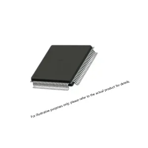
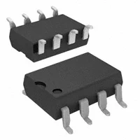
CYPRESS CY7C1380D-167AXI
- 18Mbit (512K × 36 / 1M × 18) NoBL™ pipelined synchronous SRAM with separate input/output data buses
- 167MHz clock, 3.4ns pipelined read latency — zero dead cycles between back-to-back read/write operations
- Separate I/O architecture enables simultaneous read and write data transfers on independent buses
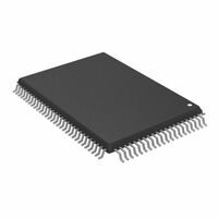
- 100-pin TQFP, industrial temperature −40°C to +85°C, 3.135V to 3.6V supply
- Obsolete lifecycle — Sparkle Electronics maintains verified lot inventory; RFQ response within 24 hours
Cypress Semiconductor (now Infineon Technologies) offered the 18Mbit NoBL™ pipelined SRAM family in two I/O configurations to address distinct board-level interface requirements: the CY7C1370D with common I/O — shared input and output data pins — and the CY7C1380D with separate I/O — independent dedicated input and output data buses. The CY7C1380D-167AXI is the separate I/O variant, available from stock at Sparkle Electronics, a specialized distributor serving defense electronics procurement teams, embedded systems engineers, and networking OEMs requiring verified sourcing of hard-to-find and obsolete SRAM with confirmed lot traceability and same-day RFQ response. The separate I/O architecture of the CY7C1380D eliminates the bus turnaround requirement that common I/O devices impose at the board level — the controller never needs to switch its data bus drivers between transmit and receive states between a write and a read, because the input and output data paths are physically separate pins. This simplifies controller interface design and can improve system throughput in implementations where bus turnaround timing represents a constraint.
The CY7C1380D-167AXI carries an obsolete lifecycle designation from Infineon. Production has been discontinued, and the global supply of this part is finite — depleting with each procurement event as active programs and repair depots continue to source remaining inventory. The AXI ordering suffix designates the 100-pin TQFP package with industrial temperature grade (−40°C to +85°C) in tube packaging. For programs in aerospace and defense embedded computing, radar and electronic warfare signal processing, and high-performance networking that specified the CY7C1380D for its separate I/O interface, securing verified stock from a traceable source is the immediate procurement priority. Contact Sparkle Electronics to confirm current inventory and initiate an RFQ.
Related Products For Your Business
Separate I/O vs. Common I/O NoBL™ SRAM: The Interface Decision That Defines Procurement Options
The distinction between the CY7C1380D (separate I/O) and the CYPRESS CY7C1370D-167AXI (common I/O) at the same 167MHz clock frequency is an interface architecture decision made at design time — one that cannot be reversed without hardware modification. Controllers and FPGAs that were interfaced to the CY7C1380D’s separate input and output buses cannot directly substitute the common I/O CY7C1370D without redesigning the PCB routing and modifying the controller’s I/O pin assignments. This interface dependency, combined with the obsolete lifecycle status of both variants, means that the CY7C1380D-167AXI procurement window is finite and closing. Procurement engineers searching for CY7C1380D-167AXI in stock, Cypress NoBL separate I/O SRAM 167MHz, CY7C1380D-167AXI obsolete stock distributor, or CY7C1380D-167AXI last-time buy will find Sparkle Electronics maintains verified lot inventory with full traceability documentation. Submit an inquiry immediately to confirm current quantity and pricing before stock position changes.
CY7C1380D-167AXI vs. CY7C1370D-167AXI: Separate I/O vs. Common I/O at 167MHz
| Parameter | CY7C1380D-167AXI | CY7C1370D-167AXI |
|---|---|---|
| Availability | In Stock at Sparkle | In Stock at Sparkle |
| Lifecycle | Obsolete | Obsolete |
| I/O Architecture | Separate I/O | Common I/O |
| NoBL™ Mode | Pipelined | Pipelined |
| Clock Frequency | 167MHz | 167MHz |
| Access Time | 3.4ns | 3.4ns |
| Capacity | 18Mbit (512K × 36) | 18Mbit (512K × 36) |
| Supply Voltage | 3.135V to 3.6V | 3.135V to 3.6V |
| Package | 100-pin TQFP | 100-pin TQFP |
| Temperature | −40°C to +85°C | −40°C to +85°C |
| Pin Compatible | No — different bus structure | No |
| Bus Turnaround | Not required (separate buses) | Required between read/write |
The separate I/O architecture of the CY7C1380D places dedicated input data pins and dedicated output data pins on physically separate package pins. The controller drives write data on the input pins and simultaneously receives read data on the output pins — with no need to tri-state, turn around, or multiplex the data bus between operations. In FPGA and ASIC implementations where separate read and write data port connections are available, the CY7C1380D’s separate I/O eliminates bus turnaround management entirely from the controller’s state machine. For controllers designed with common I/O bus architectures, the common I/O CY7C1370D is the correct original specification.
NoBL™ Pipelined Architecture at 167MHz: Throughput Characteristics
The CY7C1380D-167AXI delivers 167MHz clock frequency with a 3.4ns access time through a two-stage read pipeline. Read data registered at clock N is available at the output pins following clock N+2 — a two-cycle latency that enables the higher maximum clock frequency compared to the flow-through CYPRESS CY7C1371D-100AXI. The NoBL™ separate I/O implementation allows simultaneous read data output and write data input on every clock cycle — achieving the theoretical maximum bandwidth of the memory array without dead cycles, bus contention, or arbitration overhead. At 167MHz with 36-bit wide data and zero dead cycles, the CY7C1380D-167AXI delivers approximately 6 Gbps of effective read or write bandwidth in sustained sequential access patterns — a specification that defined reference designs for high-throughput networking and defense signal processing applications at its introduction. For broader memory and storage procurement requirements, Sparkle Electronics maintains inventory spanning active and obsolete SRAM categories across multiple organizations and interface architectures.
Frequently Asked Questions
What does CY7C1380D-167AXI decode to?
CY7C = Cypress SRAM product family prefix; 1380 = NoBL™ pipelined synchronous SRAM, 18Mbit, separate I/O architecture — the 1380 series designation differentiates from 1370 (common I/O pipelined) and 1371 (common I/O flow-through); D = D-generation silicon revision; -167 = 167MHz clock frequency; A = TQFP package type; X = RoHS/lead-free compliant; I = industrial temperature grade (−40°C to +85°C); tube packaging.
Where can I buy CY7C1380D-167AXI in stock?
Sparkle Electronics maintains verified stock of the CY7C1380D-167AXI. Given the obsolete lifecycle and finite remaining global supply, procurement teams with ongoing production or sustainment requirements should submit an RFQ without delay. Contact our team — same-day response on pricing, available quantity, lot traceability documentation, and confirmed lead time.
What is the key difference between CY7C1380D-167AXI and CY7C1370D-167AXI?
Both are 18Mbit NoBL™ pipelined synchronous SRAMs at 167MHz with identical capacity and access time. The CY7C1380D uses separate dedicated input and output data buses — the controller drives write data on input pins and simultaneously receives read data on output pins with no bus turnaround. The CY7C1370D uses a common bidirectional I/O bus that requires the controller to manage bus direction switching between read and write operations. These are not interchangeable — the pin assignments and controller interface requirements are different. Substitution requires hardware redesign.
Why does separate I/O simplify controller interface design?
With separate I/O, the controller’s read data receivers and write data drivers are permanently and independently connected to the SRAM — no tri-state control, bus direction switching, or turnaround timing management is required in the controller’s interface state machine. In FPGA implementations, this translates to simpler HDL, fewer interface states, and more deterministic timing closure. In ASIC designs, separate I/O eliminates the bus arbiter logic required for common I/O turnaround management. The trade-off is higher pin count on the SRAM — the additional dedicated I/O pins consume package pins that common I/O designs share between input and output.
What documentation is available for CY7C1380D-167AXI procurement?
Sparkle Electronics provides packing documentation, lot traceability, and country of origin certification. For programs with counterfeit risk mitigation requirements — a critical consideration for obsolete components with known open-market exposure — our team can advise on available lot history and inspection options before order placement. Documentation scope should be confirmed at inquiry stage. Contact us to initiate the documentation review process before committing to an order.
Is there a current production replacement for CY7C1380D-167AXI?
No direct pin-compatible current-production replacement exists for NoBL™ pipelined separate I/O SRAM in the 18Mbit, 100-pin TQFP configuration. Programs evaluating supply options must consider either securing sufficient verified obsolete stock for the remaining production and sustainment lifecycle, or undertaking a hardware redesign to accommodate a different SRAM architecture. Both paths carry cost and schedule implications that are best evaluated before existing stock is exhausted. Contact Sparkle Electronics to discuss current stock quantity and procurement timing for your program’s specific requirements.
Sourcing CY7C1380D-167AXI for a production or sustainment program before verified stock is depleted? Sparkle Electronics maintains confirmed inventory of obsolete Cypress NoBL™ SRAM — pipelined, flow-through, separate I/O, and common I/O variants — with full lot traceability and same-day RFQ response. Submit an inquiry now — pricing, quantity, and documentation scope confirmed within 24 hours.