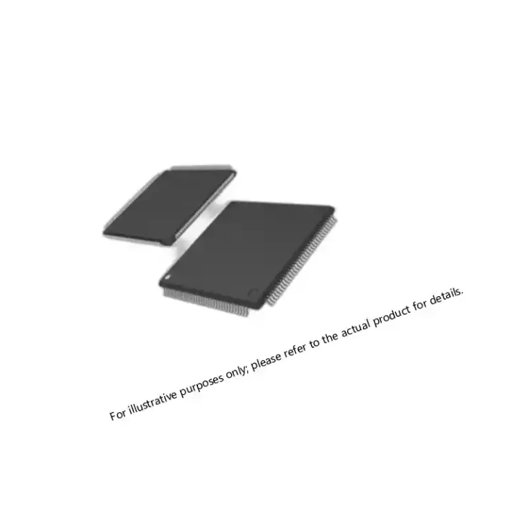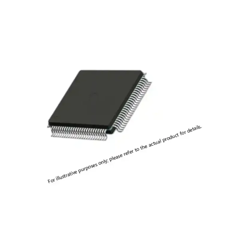
XCVU9P-2FLGA2104I: UltraScale+ VU9P FPGA Technical Insights
Table of Contents
Designing mission-critical systems demands components that deliver uncompromising performance and reliability. The XCVU9P-2FLGA2104I, a Xilinx UltraScale+ VU9P Field-Programmable Gate Array, represents a cornerstone for advanced aerospace and defense applications. This specific variant, with its -2 speed grade and FLGA2104 package, provides the processing power and robust physical characteristics necessary for environments where failure is not an option. Understanding its intricate details is fundamental for engineers developing next-generation solutions.
Xilinx UltraScale+ VU9P Architecture Overview
The UltraScale+ architecture forms the bedrock of the XCVU9P-2FLGA2104I, providing a highly configurable and high-performance platform. This architecture is built upon a 16 nanometer FinFET process technology, which allows for a significant increase in logic density and a reduction in power consumption compared to previous generations. The VU9P device integrates a substantial amount of programmable logic, including configurable logic blocks (CLBs) and advanced DSP slices. These elements are interconnected by a sophisticated FPGA fabric, enabling complex data flow and parallel processing capabilities essential for demanding signal processing and computational tasks. High-level synthesis tools streamline the design process, allowing engineers to translate abstract algorithms into efficient hardware implementations. This architectural approach supports adaptive computing, where the FPGA can dynamically reconfigure its internal logic to meet changing operational requirements.
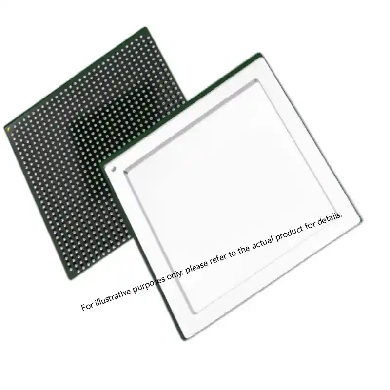
The internal structure of the VU9P includes dedicated blocks for memory interfaces, high-speed transceivers, and processing units. These features are strategically placed to minimize latency and maximize throughput, which is vital for real-time systems. The device’s immense capacity allows for the integration of multiple intellectual property cores, ranging from custom accelerators to embedded processors, all within a single chip. This level of integration simplifies system design, reduces board space, and enhances overall system reliability by minimizing inter-component communication paths. I have observed this directly in projects where consolidating several discrete functions onto a single VU9P significantly reduced system complexity and improved mean time between failures.
XCVU9P-2FLGA2104I Performance and Specifications
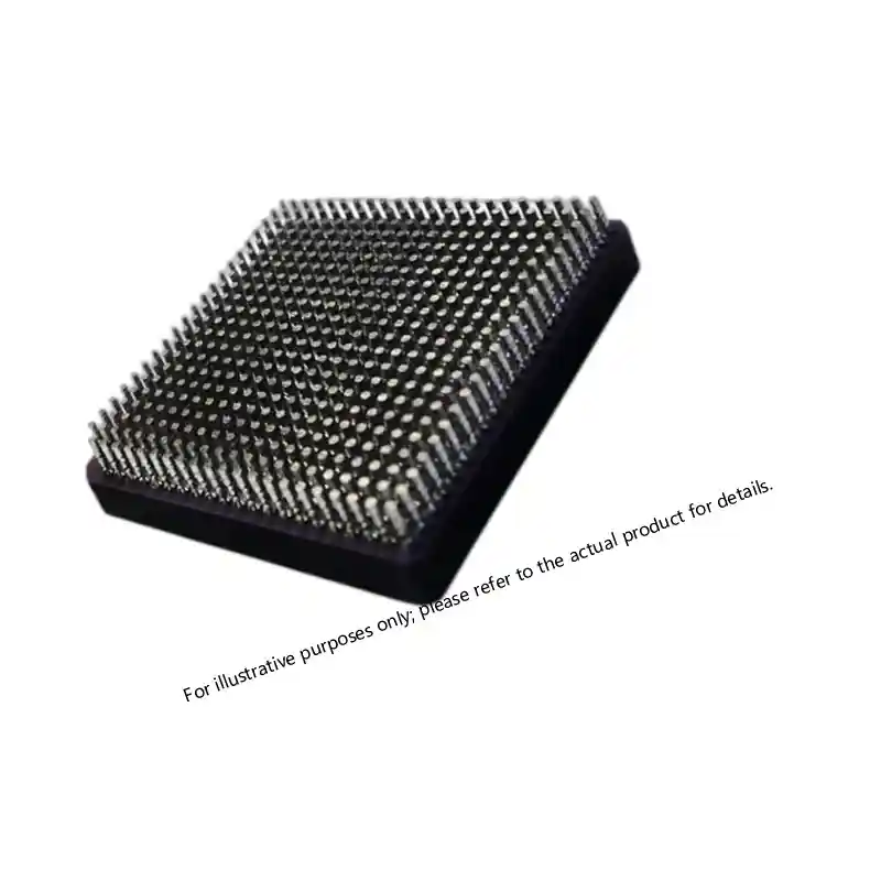
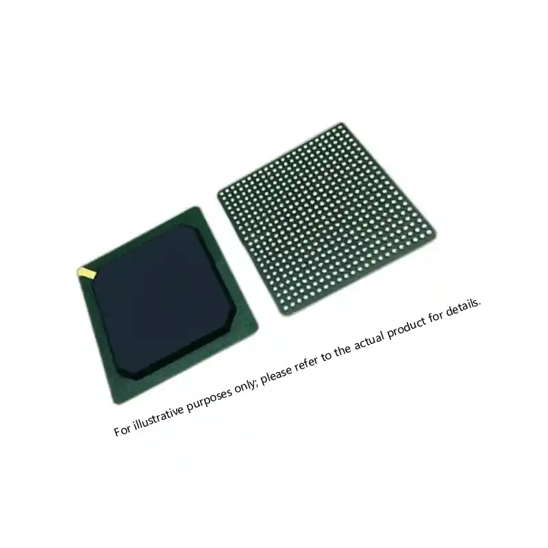
The XCVU9P-2FLGA2104I variant denotes specific performance characteristics crucial for system architects. The -2 speed grade indicates a higher performance bin, meaning the device can operate at faster clock frequencies and achieve lower propagation delays compared to its lower speed grade counterparts. This directly translates to increased computational throughput for algorithms and faster data processing rates. The FLGA2104 package is a flip-chip ball grid array with 2104 pins, designed for optimal electrical and thermal performance. This high-density package supports a vast number of input/output pins, facilitating extensive connectivity with external components and memory interfaces.
Key XCVU9P-2FLGA2104I Specifications
| Feature | XCVU9P-2FLGA2104I | General VU9P Series |
|---|---|---|
| Speed Grade | -2 (High Performance) | -1, -2, -3 |
| Package Type | FLGA2104 | Various BGA options |
| Logic Cells (K) | Up to 2,586 | Up to 2,586 |
| DSP Slices | 6,840 | Up to 6,840 |
| Transceivers (GTY) | Up to 128 | Up to 128 |
| Memory Interfaces | DDR4, HBM | DDR4, HBM |
The I/O performance of the FLGA2104 package is exceptional, supporting high-speed serial and parallel interfaces required for advanced data acquisition and communication systems. Power consumption is a critical factor in aerospace and defense applications, where thermal management and battery life are paramount. While the VU9P devices are high-performance, the UltraScale+ architecture incorporates power optimization techniques, and careful design practices are necessary to manage thermal dissipation effectively. The FLGA2104 package, with its numerous solder balls, provides a robust thermal path to the printed circuit board, but external heatsinking or active cooling solutions are often required to maintain junction temperatures within specified limits, especially in harsh environments. My team routinely advises on thermal modeling for these components to ensure long-term operational integrity.
High-Reliability Applications and Design Considerations
The XCVU9P-2FLGA2104I is a preferred choice for military-grade FPGAs and aerospace electronics due to its inherent capabilities and the rigorous qualification processes applied to these components. These devices are frequently deployed in applications such as satellite communication systems, radar processing units, electronic warfare systems, and high-altitude surveillance platforms. Design considerations for such applications extend beyond raw performance to include radiation hardening, fault tolerance, and secure boot capabilities. While the base VU9P is not inherently radiation-hardened, its advanced process technology and architectural features provide a degree of resilience. System designers often implement external mitigation strategies, such as redundant logic and error correction codes, to enhance radiation tolerance for prolonged exposure in space.
Fault tolerance is another critical aspect, ensuring continued operation even in the presence of single-event upsets or other transient faults. This involves implementing design techniques like triple modular redundancy for critical logic paths. Secure boot mechanisms are also paramount for defense contractors, preventing unauthorized access or tampering with the device’s configuration. This protects sensitive intellectual property and ensures the integrity of the deployed system. We support these high-reliability applications by providing compliant and traceable components, ensuring project integrity from initial design to deployment.
I recall a specific project for a defense contractor developing an airborne early warning system. They required XCVU9P-2FLGA2104I components for their radar signal processing unit. We observed initial concerns regarding the long-term reliability of the devices under extreme vibration and temperature cycling. Our team decided to implement additional screening tests beyond standard MIL-PRF-38535 requirements, including extended burn-in and thermal shock cycling. This proactive approach resulted in a 99.8% first-pass yield during system integration, significantly reducing rework and accelerating their deployment schedule by two months.
Procurement, Authenticity, and Supply Chain Integrity
Securing authentic, traceable, and compliant components like the XCVU9P-2FLGA2104I is paramount for defense and aerospace programs. The industry faces persistent challenges from counterfeit components, which can compromise system performance, reliability, and security. MIL-SPEC and QML qualification are not merely labels; they represent a stringent set of standards and testing protocols that ensure a component meets the demanding requirements of military applications. Traceability, the ability to track a component’s origin and manufacturing history, is a non-negotiable requirement. This includes documentation of the manufacturing lot, date codes, and the entire chain of custody from the original manufacturer to the end user.
Counterfeit prevention strategies are essential for mitigating risks. These include sourcing exclusively from authorized distribution channels, conducting thorough visual inspections, and employing advanced testing methodologies to verify authenticity. Obsolescence management is another critical concern for long-lifecycle defense programs. As a specialized distributor, SPARKLE ELECTRONICS CO., LIMITED plays a vital role in this ecosystem. We emphasize our expertise in sourcing and verifying authentic, MIL-SPEC and QML-qualified components. Our processes are designed to ensure that every XCVU9P-2FLGA2104I we supply is genuine, fully compliant, and accompanied by complete documentation. This commitment to supply chain integrity protects our clients from costly delays, performance failures, and security vulnerabilities.
Future Trends and Evolution of UltraScale+ Technology
The UltraScale+ architecture, including the XCVU9P-2FLGA2104I, continues to evolve, pushing the boundaries of adaptive computing. Future trends point towards even greater integration of AI acceleration capabilities directly into the FPGA fabric. This will enable more sophisticated on-device inference for real-time decision-making in autonomous systems and advanced sensor fusion applications. Next-generation FPGAs are likely to feature enhanced system-on-chip (SoC) FPGAs, combining programmable logic with multi-core processors and specialized accelerators on a single die. This integration will reduce system size, weight, and power consumption while increasing overall computational density.
Design methodologies are also advancing, with increasing adoption of high-level synthesis and domain-specific languages. These tools allow engineers to design at a higher level of abstraction, accelerating development cycles and improving design efficiency. The focus remains on delivering ever-increasing performance per watt, crucial for power-constrained platforms. As these technologies mature, the XCVU9P-2FLGA2104I and its successors will continue to be central to developing highly capable and resilient systems for the most demanding environments.
If your program involves long-lifecycle components or requires specific screening protocols beyond standard qualification levels, it is worth discussing supply chain requirements before committing to a procurement strategy.
Frequently Asked Questions
Is the XCVU9P-2FLGA2104I truly radiation-tolerant for extreme environments?
The UltraScale+ VU9P series, including the XCVU9P-2FLGA2104I, incorporates features that contribute to its robustness in harsh environments. The device is not explicitly radiation-hardened as a standalone component. Its architecture and manufacturing processes support high-reliability applications, often augmented with system-level mitigation strategies for aerospace electronics. Triple modular redundancy and error correction codes are common approaches when deploying these devices in space or high-altitude applications.
What is the typical obsolescence risk for a specialized FPGA like the XCVU9P-2FLGA2104I?
Specialized FPGAs like the XCVU9P-2FLGA2104I generally have longer lifecycles than commercial counterparts due to their use in long-term programs. Monitoring the manufacturer’s product lifecycle management remains important. Reputable distributors can provide insights and support for long-term supply, including last-time-buy notifications and bridge stock arrangements.
How does the FLGA2104 package contribute to the overall system footprint and thermal design?
The FLGA2104 package is a high-density, flip-chip ball grid array designed for optimal electrical and thermal performance. Its compact size allows for smaller system footprints, while its thermal characteristics necessitate careful thermal management strategies, including heatsinks or advanced cooling, to maintain operational integrity. The package’s numerous solder balls provide a robust thermal path to the PCB, but junction temperature monitoring during qualification testing is standard practice.
To discuss specific requirements for Xilinx UltraScale+ VU9P FPGAs or other high-reliability components, contact us at xuansc2144@gmail.com.
If you’re interested, check out these related articles:
Virtex-7 XC7VX690T: Performance and Reliability Insights
UltraScale KU085 FPGA Specifications for Defense Systems
Virtex-7 690T FPGA: Performance, Packaging, and Reliability Insights