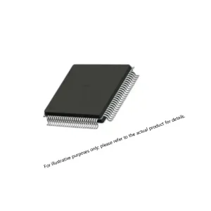

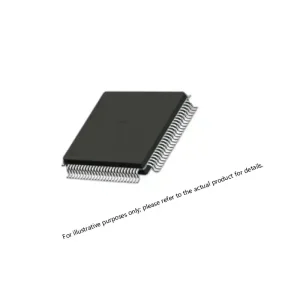
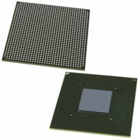
ALTERA 5AGXMB3G4F35I5N
- 3.5 million logic elements for mid-range signal processing
- Up to 768 GMACs digital signal processing performance
- 28 Gbps transceivers for high-speed data transmission
- Radiation-tolerant design for aerospace environments
- Extended temperature range: -40°C to +100°C
Related Products For Your Business
The Altera 5AGXMB3G4F35I5N is an Arria V GX FPGA — 136,880 ALMs (≈362K logic elements), 1,726 M10K memory blocks, 1,045 variable-precision DSP blocks, transceivers up to 10.3125 Gbps — in the 1,152-pin F35 FBGA package, industrial temperature grade I5. It occupies the mid-range of the Arria V GX B-series, delivering substantially more logic and DSP resources than the 5AGXB1 while remaining in the same F35 package as the higher-density 5AGXBB7D4F35I5N, enabling PCB reuse across program phases or risk reduction from a lower-density pilot to the full B7 in production.
5AGXMB3 vs. 5AGXBB7 — Resource Comparison
| Resource | 5AGXMB3 (this device) | 5AGXBB7D4F35I5N |
|---|---|---|
| ALMs | 136,880 | 190,240 |
| Logic Elements (K) | 362 | 504 |
| M10K Memory Blocks | 1,726 | 2,414 |
| Total Block Memory (KByte) | 17,260 | 24,140 |
| Variable-Precision DSP Blocks | 1,045 | 1,156 |
| 18×19 Multipliers | 2,090 | 2,312 |
| Fractional PLLs | 12 | 16 |
| GPIO | 704 | 704 |
| Package | F35 (1,152-pin) | F35 (1,152-pin) |
| Speed Grade | I5 (industrial) | I5 (industrial) |
The 5AGXMB3 is the preferred choice when the 5AGXBB7’s 190K ALMs exceed actual design utilization by a significant margin — a common situation in early-phase signal processing FPGA designs where 60–70% utilization is the practical ceiling before timing closure becomes difficult. By selecting the mid-density B3, the designer preserves PCB compatibility with the B7 (identical F35 footprint, same power pins, same configuration pins) while reducing BOM cost and static power consumption. The 28nm low-power process delivers the lowest static power in the mid-range transceiver FPGA category, with hard IP for PCIe Gen1/Gen2/Gen3, GbE, SRIO, and CPRI reducing dynamic power versus equivalent soft implementations.
FAQ
What is the difference between 5AGXMB3G4F35I5N and 5AGXBB7D4F35I5N?
Logic density: 136,880 ALMs vs. 190,240 ALMs. The B3 has fewer M10K blocks (1,726 vs. 2,414) and DSP blocks (1,045 vs. 1,156), but shares the same F35 package, I5 speed grade, transceiver architecture, and hard IP blocks.
Are these two devices pin-compatible on the same PCB?
Yes — both use the F35 (1,152-pin FBGA) package with identical power, configuration, and dedicated pin assignments, enabling vertical migration between density grades without PCB redesign.
What is the practical use case for choosing B3 over B7?
When design utilization is projected at 50–70% of the B7 capacity, specifying the B3 reduces unit cost and static power while maintaining a clear upgrade path to the B7 if design scope expands. Arria V GX vertical migration is documented in Intel’s device handbook.
What transceiver protocol hard IP is included?
PCIe Gen1/Gen2/Gen3 (x1 to x8 configurations), Gigabit Ethernet MAC, Serial RapidIO, CPRI, and GPON. All standard and proprietary serial protocols from 611 Mbps to 10.3125 Gbps are supported.
What does the I5 speed grade mean for defense applications?
I5 is the slower of the two industrial speed grades (I3 being faster). It covers −40°C to +100°C junction temperature and is the appropriate grade for defense systems requiring below-0°C operation where commercial grades (C4, C5, C6) are not rated.
What design tools support this device?
Intel Quartus Prime (all editions), including IP Library access for DSP Builder, JESD204B, OpenCL SDK, and all Altera MegaCore IP functions. ModelSim-Altera and Questa support simulation. All Arria V GX devices are supported in the current Quartus Prime release.