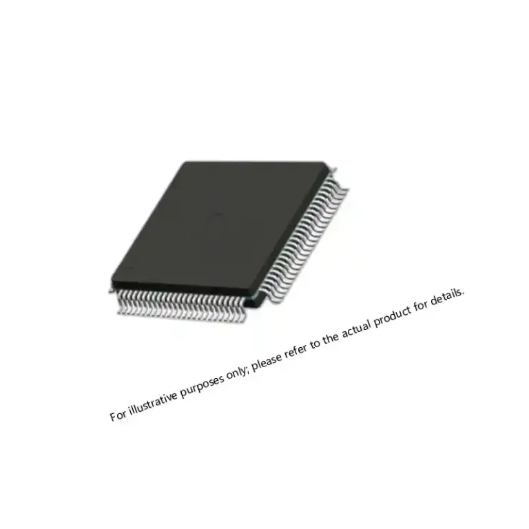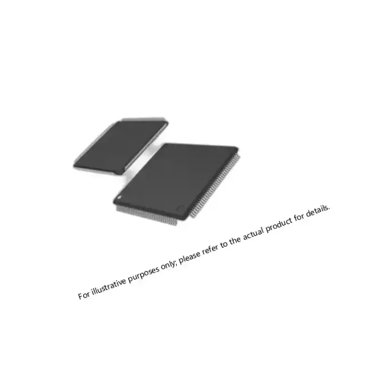
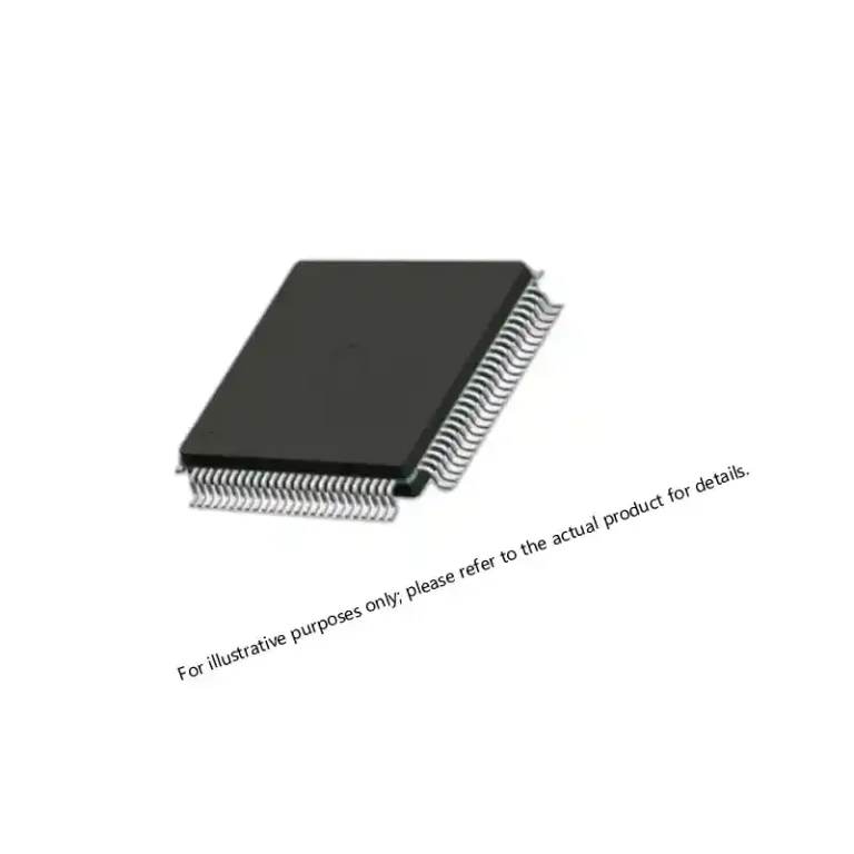
3D Packaging for Military Hi-Rel ICs: What Defense Programs Require
Table of Contents
- Why Defense Programs Adopt 3D Packaging for Military ICs
- Qualification Standards for 3D Packaged Military ICs
- Multi-Chip Module and System-in-Package Configurations
- Sourcing 3D Packaged Military ICs: Lead Times and Availability
- When 3D Packaging Creates More Risk Than It Solves
- How Sparkle Electronics Supports 3D Packaging Procurement
- Common Questions About 3D Packaging for Military Applications
- What distinguishes 3D packaging from 2.5D integration in military ICs?
- How do thermal constraints affect 3D package selection for defense systems?
- What qualification testing applies specifically to 3D packaged military ICs?
- Can existing military designs migrate to 3D packaging without redesign?
- What lead times should programs expect for QML-qualified 3D packages?
- Sources and Further Reading
Defense electronics programs face a fundamental constraint: mission-critical systems demand more processing power, faster data conversion, and greater memory density while operating within fixed volume and weight budgets. Traditional single-die packaging cannot deliver the integration density required for next-generation radar signal processors, electronic warfare systems, and satellite payloads. 3D packaging and advanced packaging technologies address this gap by stacking multiple die vertically or integrating heterogeneous components within a single package, but qualifying these structures for military environments introduces verification challenges that commercial applications never encounter.
The shift toward 3D packaging in military ICs reflects a broader industry trajectory. According to Yole Développement’s 2024 Advanced Packaging Report, the global advanced packaging market reached $44.3 billion in 2023, with 2.5D and 3D integration segments growing at 22% annually. Defense programs increasingly adopt these technologies not because they follow commercial trends, but because SWaP-C (Size, Weight, Power, and Cost) optimization has become a program requirement rather than a design preference.
Why Defense Programs Adopt 3D Packaging for Military ICs
The operational case for 3D packaging in defense applications centers on three measurable outcomes: reduced interconnect length, improved signal integrity, and higher functional density per unit volume.
Vertical die stacking shortens the electrical path between components. In a traditional multi-chip module with side-by-side die placement, signal traces between an FPGA and adjacent memory may span 15 to 25 millimeters. A 3D stacked configuration using through-silicon vias (TSVs) reduces this distance to under 100 micrometers. The result is lower parasitic capacitance, reduced signal propagation delay, and decreased power consumption for high-speed interfaces.
For radar signal processing applications, this matters directly. A phased array radar system processing 16 simultaneous beams requires sustained memory bandwidth exceeding 200 GB/s. Achieving this bandwidth with conventional packaging demands multiple parallel memory channels, each consuming board area and adding weight. High-bandwidth memory (HBM) stacked on a processing die delivers equivalent bandwidth in a fraction of the footprint.
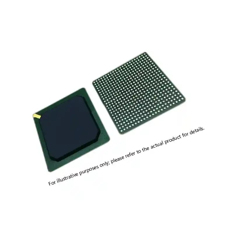
The thermal management challenge in 3D packaging is real but manageable. Stacking die increases power density per unit area, concentrating heat generation. Military-grade 3D packages address this through several mechanisms: thinned die (typically 50 to 100 micrometers versus 750 micrometers for standard die), thermal interface materials with conductivity exceeding 5 W/mK, and package designs that provide direct thermal paths from the die stack to the heat spreader.
| Packaging Approach | Typical Interconnect Density | Thermal Resistance | Volume Efficiency |
|---|---|---|---|
| Traditional MCM | 100–200 I/O per cm² | 0.5–1.0 °C/W | Baseline |
| 2.5D Interposer | 1,000–5,000 I/O per cm² | 0.3–0.6 °C/W | 2–3× improvement |
| 3D TSV Stack | 10,000+ I/O per cm² | 0.4–0.8 °C/W | 4–8× improvement |
Qualification Standards for 3D Packaged Military ICs
Military qualification of 3D packaged ICs follows established frameworks but requires additional verification steps that account for the unique failure modes these structures introduce.
MIL-PRF-38535 remains the governing specification for Class Q (space) and Class V (military) qualified microcircuits. The standard’s test methods, defined in MIL-STD-883, apply to 3D packages with specific attention to tests that stress vertical interconnects. Test Method 2019 (die shear) and Test Method 2011 (bond strength) verify the mechanical integrity of die attach in stacked configurations. Thermal cycling per Test Method 1010 evaluates the reliability of TSV structures under repeated temperature excursions from -55°C to +125°C.
The Defense Logistics Agency’s Qualified Manufacturers List (QML) process for 3D packages requires manufacturers to demonstrate process control over several parameters that do not apply to conventional packaging: TSV fill uniformity, micro-bump coplanarity, underfill void content, and interposer warpage. These parameters directly affect long-term reliability in military environments.
JEDEC’s JEP158 guideline provides a framework for 3D package reliability testing that supplements MIL-STD-883. The guideline addresses failure mechanisms specific to 3D integration: TSV stress-induced cracking, micro-bump electromigration, and die-to-die delamination. Programs requiring extended mission life (15+ years for satellite applications) should confirm that qualification testing addresses these mechanisms explicitly.
Radiation hardness assurance for 3D packages presents additional complexity. Total ionizing dose (TID) and single-event effects (SEE) testing must account for the shielding effect of stacked die. A memory die positioned beneath a logic die receives partial shielding from incident radiation, potentially masking vulnerabilities that would appear in standalone testing. Qualification protocols should specify testing of individual die as well as the assembled stack.
Multi-Chip Module and System-in-Package Configurations
Multi-chip modules (MCMs) and system-in-package (SiP) solutions represent the most mature advanced packaging technologies for military applications. These approaches integrate multiple die within a single package without requiring TSV technology, offering a lower-risk path to increased integration density.
MCM configurations typically place die side-by-side on a common substrate, with interconnections provided by substrate metallization or wire bonds. This approach works well for combining die from different process nodes or different foundries. A typical military MCM might integrate a rad-hard FPGA from one manufacturer with high-speed ADCs from another and memory from a third, all within a hermetically sealed ceramic package.
The substrate technology significantly affects MCM performance. Thick-film ceramic substrates (HTCC or LTCC) provide excellent hermeticity and thermal performance but limit routing density to approximately 100 lines per centimeter. Thin-film substrates on ceramic or silicon carriers increase routing density by an order of magnitude, enabling higher I/O count die integration.
SiP configurations extend the MCM concept by incorporating passive components, filters, and discrete devices within the package. A military SiP for a software-defined radio application might include the RF front-end, digital baseband processor, power management, and filtering within a single package. This level of integration reduces board-level assembly complexity and eliminates interconnect parasitics that degrade RF performance.
| Configuration | Die Count | Typical Applications | Qualification Path |
|---|---|---|---|
| Standard MCM | 2–4 die | Mixed-signal systems, sensor interfaces | MIL-PRF-38535 Class K/Q/V |
| High-Density MCM | 5–12 die | Signal processors, communications | MIL-PRF-38535 with extended testing |
| SiP | 3–8 die + passives | RF systems, power converters | MIL-PRF-38535 or MIL-PRF-19500 |
Sourcing 3D Packaged Military ICs: Lead Times and Availability
The supply chain for 3D packaged military ICs differs substantially from standard military components. Production volumes are lower, qualification cycles are longer, and the number of qualified sources is limited.
Lead times for QML-qualified 3D packages typically range from 26 to 52 weeks for standard products, extending to 78 weeks or longer for custom configurations. These timelines reflect the complexity of the assembly process, the limited number of facilities with military-grade 3D packaging capability, and the extended qualification testing required.
Programs should evaluate several factors when specifying 3D packaged ICs:
Die source qualification: The individual die within a 3D package may come from different foundries with different qualification status. A package containing a QML-qualified FPGA and a non-QML memory die does not automatically inherit QML status for the assembly. Confirm the qualification level of each die and the assembly process independently.
Second-source availability: The specialized nature of 3D packaging limits second-source options. Programs with long production runs or sustainment requirements should assess whether alternative assembly sources exist and whether design data rights permit requalification at a second facility.
Die banking and wafer storage: For programs with 15+ year lifecycles, consider procuring die or wafers for storage before the component reaches end-of-life. 3D assembly can be performed on stored die, but the die must be properly stored (typically in nitrogen at controlled temperature and humidity) to maintain bondability.
Documentation requirements: 3D packages require additional documentation beyond standard military IC procurement. Request assembly flow diagrams, TSV or micro-bump inspection criteria, and underfill cure profiles. These documents support failure analysis if field issues arise.
When 3D Packaging Creates More Risk Than It Solves
Not every application benefits from 3D packaging. The technology introduces failure modes that do not exist in conventional packages, and the qualification history is shorter than for established packaging approaches.
Programs should evaluate 3D packaging critically when:
Thermal margins are tight: 3D stacking concentrates heat generation. If the system thermal design already operates near its limits, adding a 3D package may require redesigning the cooling system. The net SWaP benefit disappears if the package requires a larger heat sink or active cooling.
Radiation requirements are extreme: TSV structures and thin die introduce radiation response characteristics that differ from bulk silicon. For applications requiring TID tolerance above 100 krad(Si) or SEE immunity to heavy ions with LET above 40 MeV·cm²/mg, confirm that the specific 3D package has been characterized to these levels.
Production volumes are very low: The non-recurring engineering cost for a custom 3D package can exceed $500,000, with qualification adding another $200,000 to $400,000. For programs procuring fewer than 100 units, the per-unit cost may not justify the integration benefits.
Long-term sustainment is required without design data rights: If the program cannot access the assembly design data, sustaining a 3D packaged IC through a 20-year lifecycle becomes dependent on a single source. Evaluate whether the manufacturer’s long-term viability and commitment to military markets supports this dependency.
The decision to adopt 3D packaging should follow a structured trade study comparing the SWaP-C benefits against the qualification cost, supply chain risk, and technical maturity for the specific application. Programs that skip this analysis often discover the limitations after design commitment, when changing direction is expensive.
How Sparkle Electronics Supports 3D Packaging Procurement
Defense programs evaluating 3D packaged military ICs face a sourcing challenge: the components are specialized, the supply base is limited, and the documentation requirements are extensive. Sparkle Electronics maintains relationships with manufacturers producing QML-qualified MCMs, SiPs, and 3D stacked packages, providing access to components that may not appear in standard distribution channels.
Our inventory includes advanced packaging solutions from manufacturers supporting military and space applications. For programs requiring custom 3D configurations, we coordinate with assembly facilities to define specifications, establish qualification test plans, and manage the procurement timeline from design through delivery.
If your program is evaluating 3D packaging options or needs to source specific MCM or SiP configurations, share your requirements with our team at xuansc2144@gmail.com. We can confirm availability, provide lead time estimates, and identify qualification documentation for the components you need.
Common Questions About 3D Packaging for Military Applications
What distinguishes 3D packaging from 2.5D integration in military ICs?
The distinction centers on vertical versus lateral integration. 2.5D packaging places multiple die side-by-side on a silicon or glass interposer, with the interposer providing high-density routing between die. 3D packaging stacks die vertically, using through-silicon vias to create direct electrical connections between layers. Military applications use both approaches depending on the integration requirement: 2.5D works well for combining logic and memory with high bandwidth, while 3D stacking maximizes volume efficiency when thermal constraints permit. The qualification approach differs as well, since 3D stacking introduces stress concentrations at TSV locations that require specific reliability testing.
How do thermal constraints affect 3D package selection for defense systems?
Thermal management becomes the primary design constraint in most 3D military applications. Stacking die increases power density per unit area, and the thermal resistance from the top die to the package exterior is higher than for a single-die package. Successful implementations use thinned die (50–100 μm) to reduce thermal resistance, high-conductivity die attach materials, and package designs that provide direct thermal paths to the heat spreader. Programs should request thermal characterization data from the manufacturer and validate thermal performance in the intended operating environment before committing to a 3D solution.
What qualification testing applies specifically to 3D packaged military ICs?
MIL-STD-883 test methods apply to 3D packages with additional attention to tests that stress the vertical interconnects. Thermal cycling (Test Method 1010) evaluates TSV reliability under repeated temperature excursions. Die shear (Test Method 2019) verifies die attach strength in stacked configurations. For packages using micro-bumps, electromigration testing per JEDEC standards supplements the MIL-STD-883 requirements. Radiation testing should characterize both the individual die and the assembled stack, since shielding effects can mask vulnerabilities. Programs with extended mission life requirements should confirm that qualification testing addresses the failure mechanisms specific to 3D integration.
Can existing military designs migrate to 3D packaging without redesign?
Migration feasibility depends on the specific design and the 3D packaging approach. Drop-in replacement is rarely possible because 3D packages have different pinouts, thermal characteristics, and electrical parasitics than their predecessors. However, functional migration is often straightforward when the design uses standard interfaces. A system using discrete FPGA and memory components can migrate to an FPGA with stacked HBM if the FPGA vendor offers a pin-compatible or footprint-compatible 3D variant. The design effort focuses on board-level changes rather than FPGA logic redesign. Confirm interface compatibility and thermal requirements early in the migration assessment.
What lead times should programs expect for QML-qualified 3D packages?
Standard QML-qualified 3D packages typically require 26 to 52 weeks from order to delivery, reflecting the specialized assembly process and extended testing requirements. Custom configurations or new qualifications extend this timeline to 78 weeks or longer. Programs can reduce lead time risk by identifying components early in the design phase, establishing blanket orders for production quantities, and considering die banking for long-lifecycle programs. Working with a distributor that maintains relationships with 3D packaging manufacturers can also improve visibility into production schedules and allocation priorities. If your timeline is constrained, reach out with your part numbers and quantities so we can confirm current availability.
Sources and Further Reading
Yole Développement — Advanced Packaging Report, 2024
JEDEC — JEP158: 3D Chip Stack Reliability Guideline
If you’re interested, check out these related articles:
XCKU085 UltraScale FPGA: Performance for Critical Systems
Virtex-7 690T FPGA: Performance, Packaging, and Reliability Insights
Virtex-7 XC7VX690T: Performance, Reliability, and Integration
Virtex-7 XC7VX690T: Performance and Reliability Insights
XC7VX485T FPGA: Virtex-7 Performance for Defense