Virtex-7 XC7VX690T: Performance, Reliability, and Integration
Table of Contents
- What the XC7VX690T Architecture Actually Provides
- Why the -2 Speed Grade and FFG1930 Package Combination Works
- How Procurement Failures Happen and How to Prevent Them
- Where the XC7VX690T Fits in Defense and Aerospace Systems
- Managing Long-Term Availability for Extended Program Lifecycles
- Frequently Asked Questions
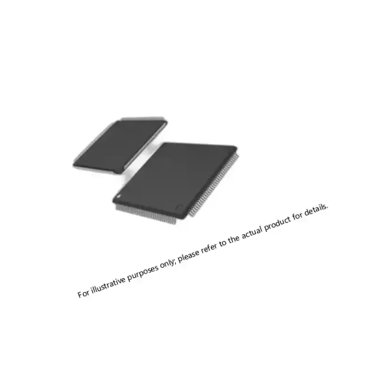
The Virtex-7 XC7VX690T FPGA delivers the logic density and I/O bandwidth that radar, electronic warfare, and satellite communication systems require when processing multiple high-speed data streams simultaneously. This device, built on Xilinx’s 28nm process, packs 693,120 logic cells, 52.9 Mb of Block RAM, and 3,600 DSP slices into a single package. The -2 speed grade and FFG1930 flip-chip ball grid array make it a practical choice for designs where timing closure, thermal management, and long-term availability all matter.
What the XC7VX690T Architecture Actually Provides
The Virtex-7 XC7VX690T sits at the high end of Xilinx’s 28nm FPGA lineup. Its logic capacity supports parallel processing pipelines that would require multiple smaller devices to replicate, and the 96 transceivers running up to 13.1 Gb/s each handle the backplane and sensor interfaces common in defense platforms.
| Feature | XC7VX690T Specification | Practical Impact |
|---|---|---|
| Logic Cells | 693,120 | Supports multiple processing pipelines in a single device |
| Block RAM (Mb) | 52.9 | Reduces external memory dependencies for latency-sensitive algorithms |
| DSP Slices | 3,600 | Handles FFT, FIR, and beamforming without fabric bottlenecks |
| Transceivers (Gb/s) | 96 (up to 13.1) | Connects directly to high-speed ADCs and backplane interfaces |
| I/O Pins | 1,200 | Accommodates multiple parallel buses and control interfaces |
The 28nm process delivers better performance per watt than the 40nm Virtex-6 generation, which matters when the FPGA sits inside a sealed enclosure with limited cooling capacity. The routing fabric bandwidth keeps up with the logic density, so designs that utilize most of the available resources can still meet timing without excessive placement iterations.
Why the -2 Speed Grade and FFG1930 Package Combination Works
Speed grades in Xilinx FPGAs indicate the worst-case propagation delays through the logic and routing. The -2 grade offers faster timing than -1 while consuming less power than -3, landing in the range where most high-performance designs can close timing without excessive power budgets. For a device this size, that balance matters because thermal headroom directly affects reliability.
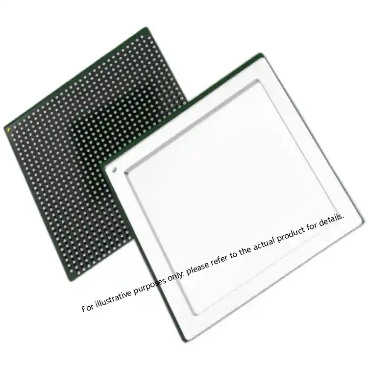
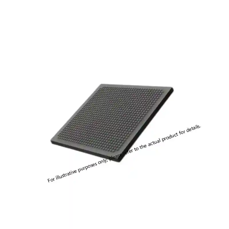
The FFG1930 package uses a flip-chip ball grid array with 1930 solder balls. This construction places the die face-down against the package substrate, which shortens the electrical path between the die and the board and improves the thermal path from the die to the heat sink. The reduced inductance helps maintain signal integrity on the high-speed transceivers, and the direct thermal connection keeps junction temperatures manageable during sustained operation.
| Package Characteristic | FFG1930 Implementation | Design Consequence |
|---|---|---|
| Pin Count | 1930 | Supports full I/O utilization without pin-limited designs |
| Construction | FCBGA | Lower inductance on power and signal paths |
| Thermal Path | Die-to-ball direct | Heat sink attaches to package bottom for efficient cooling |
| Mechanical Robustness | Underfill compatible | Withstands vibration and thermal cycling in deployed systems |
Board layout for the FFG1930 requires attention to power plane impedance and decoupling capacitor placement. The power delivery network needs to supply clean voltage rails to hundreds of simultaneous switching outputs, and the high transceiver count means careful attention to reference clock distribution and channel-to-channel skew.
How Procurement Failures Happen and How to Prevent Them
Sourcing military-grade FPGAs involves more than finding a part number match. Counterfeit components enter the supply chain through various paths, and a non-authentic device can fail in ways that only appear under specific operating conditions, making root cause analysis difficult after integration.
A radar system upgrade project illustrates the risk. The program needed XC7VX690T devices urgently, and several distributors offered stock. One supplier’s documentation showed date codes that did not match the expected manufacturing timeline for the lot numbers provided. Further investigation revealed the parts came from an unauthorized source with no traceability to Xilinx’s production facilities. Rejecting that supplier avoided integrating devices that might have failed qualification testing or degraded unpredictably in the field.
The verification process that caught this discrepancy included requesting Certificate of Conformance documentation, cross-referencing date codes against known manufacturing schedules, and confirming the supplier’s authorization status with the original manufacturer. For programs where a component failure could compromise mission success, this level of scrutiny is not optional.
Where the XC7VX690T Fits in Defense and Aerospace Systems
The logic density and transceiver count make this FPGA suitable for applications that combine high-bandwidth sensor interfaces with computationally intensive signal processing. Electronic warfare systems use devices like the XC7VX690T to perform real-time spectrum analysis across wide frequency ranges, identifying and characterizing signals faster than software-based approaches allow. Satellite communication terminals use the DSP slices for modulation and demodulation while the transceivers handle the high-speed links to RF front ends.
System-on-chip implementations benefit from the ability to integrate soft processor cores, custom accelerators, and peripheral interfaces within a single device. This reduces board complexity and eliminates inter-chip communication bottlenecks that would otherwise limit throughput. The tradeoff is design complexity, which requires thorough verification through simulation, formal methods, and hardware testing before the design goes into production.
Managing Long-Term Availability for Extended Program Lifecycles
Defense programs often operate equipment for 20 years or more, which creates a mismatch with semiconductor product lifecycles. Xilinx will eventually discontinue the Virtex-7 family, and programs that depend on the XC7VX690T need strategies to address that eventuality.
Effective obsolescence management starts with lifecycle monitoring. Tracking manufacturer announcements and distributor inventory levels provides early warning when a device approaches end-of-life. Last-time buy opportunities allow programs to secure sufficient inventory for projected needs, though this requires accurate forecasting of production quantities and failure rates over the remaining program life.
When last-time buy is not practical, identifying form-fit-function replacements becomes necessary. Newer FPGA families may offer compatible devices, though design migration requires re-verification and potentially re-qualification. Maintaining access to the original design files, development tools, and any third-party IP cores used in the design makes this migration feasible when it becomes necessary.
If your program requires XC7VX690T devices or other high-reliability FPGAs, discussing your long-term quantity projections and delivery schedule early helps ensure availability throughout your program lifecycle.
Frequently Asked Questions
What makes the XC7VX690T-2FFG1930I suitable for aerospace applications?
The device combines high logic density for complex algorithms, sufficient DSP resources for real-time signal processing, and a package designed for efficient thermal management in constrained enclosures. The -2 speed grade provides the timing performance most aerospace designs require without excessive power consumption. These characteristics match the computational demands and environmental constraints typical of aerospace platforms.
Which design tools support Virtex-7 FPGA development?
Xilinx’s Vivado Design Suite handles synthesis, implementation, and timing analysis for Virtex-7 devices. The toolchain includes simulation capabilities, IP integrator for block-based design, and hardware debugging features. Programs using Virtex-7 FPGAs should maintain access to compatible Vivado versions throughout the product lifecycle, as newer tool versions may drop support for older device families.
How does the -2 speed grade affect power consumption compared to other grades?
The -2 grade typically consumes less power than -3 for equivalent designs because it operates at lower supply voltages for the same timing performance. However, actual power consumption depends heavily on the specific design, including clock frequencies, logic utilization, and I/O activity. Power estimation during design and measurement on prototype hardware provide more accurate numbers than speed grade comparisons alone.
Navigating high-reliability component procurement requires attention to authenticity, traceability, and long-term program support. To discuss your specific FPGA requirements and ensure your systems remain supportable throughout their operational life, contact us at xuansc2144@gmail.com.
If you’re interested, you may want to read the following articles:
XC7VX485T Virtex-7 FPGA: Performance and Sourcing for Defense
A1020B-PG84B ACT2 FPGA: Specs, Sourcing, and Availability