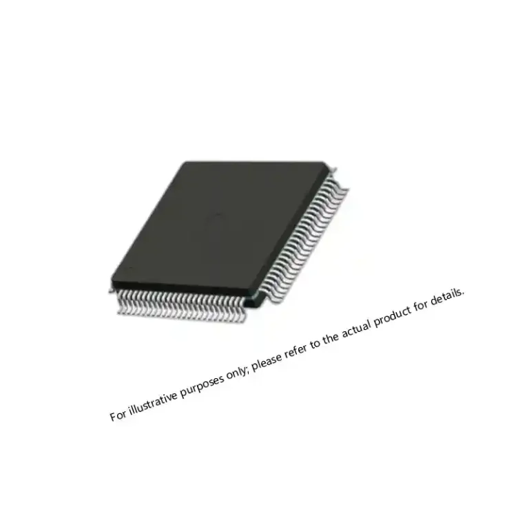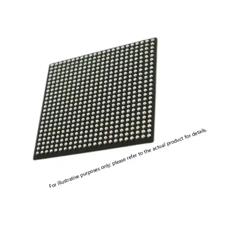
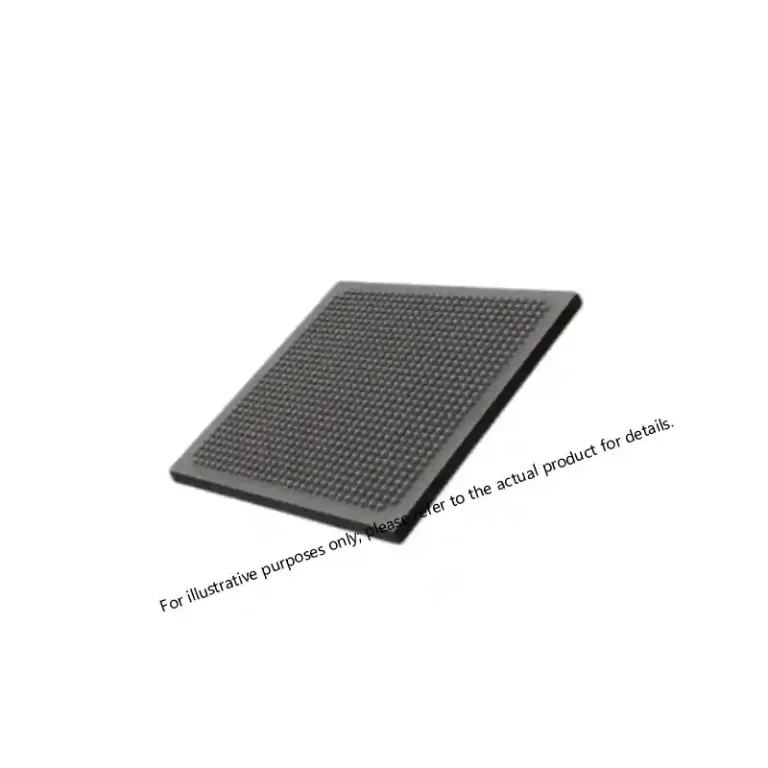
XCKU085 UltraScale FPGA: Performance for Critical Systems
Table of Contents
Field Programmable Gate Arrays remain the go-to solution when a system needs to process data at wire speed while retaining the option to change its logic after deployment. The Xilinx XCKU085 UltraScale FPGA sits in the upper tier of that category, built for workloads where throughput and reconfigurability both matter. Radar front-ends, software-defined radios, and high-speed data acquisition rigs are typical homes for this device. What follows covers the architecture, the part-number breakdown, application fit, environmental limits, and the sourcing realities that come with any high-reliability FPGA.
How the XCKU085 UltraScale Architecture Handles Heavy Workloads
The Kintex UltraScale family uses TSMC’s 20 nm process node, which gives the XCKU085 roughly 830,000 logic cells in a footprint that would have required a much larger die on older nodes. Configurable logic blocks still form the core fabric, but the interesting story is what surrounds them.
DSP slices, 3,960 of them in this device, are hardened multiply-accumulate engines. A single slice can execute an 18×25-bit multiply plus a 48-bit accumulate in one clock cycle. Chaining slices together builds FIR filters, FFT butterflies, or matrix operations without burning general logic. For a radar pulse-compression stage or a polyphase channelizer, these slices do most of the arithmetic while the CLBs handle control and routing.
Block RAM totals 43.2 Mb, distributed across the die in 36 Kb tiles that can be configured as dual-port memory, FIFOs, or ROM. Placing memory close to the logic that consumes it keeps latency low and avoids external memory bottlenecks for intermediate buffers.
High-speed transceivers, rated to 16.3 Gb/s per lane, handle off-chip communication. A typical design might aggregate four lanes into a 64 Gb/s link to a backplane switch or a high-speed ADC interface. The transceivers include equalization and clock-data recovery on-chip, which simplifies board design when trace lengths vary.
Taken together, the architecture lets a single FPGA replace what used to require a DSP chip, an external memory controller, and a separate serializer-deserializer. Board area shrinks, and so does the number of solder joints that can fail in a vibration environment.
What the XCKU085-2FLVB1760E Part Number Actually Tells You
Xilinx part numbers pack a lot of information into a short string. Breaking down XCKU085-2FLVB1760E piece by piece:
XCKU085 identifies the device as a Kintex UltraScale with 830,000 logic cells. The KU prefix distinguishes it from the higher-end VU (Virtex UltraScale) and the lower-cost AU (Artix UltraScale+) families.
The -2 speed grade means the device has been characterized and binned for faster timing. Compared to a -1 part, the -2 grade allows higher Fmax on registered paths and tighter setup margins on high-speed I/O. In practice, a -2 device might close timing at 450 MHz where a -1 device tops out around 400 MHz for the same logic. That 12% headroom can be the difference between meeting a real-time deadline and missing it.
FLVB1760 describes the package. FL indicates a flip-chip BGA with a 1.0 mm ball pitch. The V denotes a specific ball map variant, and B1760 means 1,760 balls. A high ball count provides enough power and ground connections to keep supply impedance low and enough signal pins to route wide parallel buses or multiple transceiver lanes without running out of I/O.
The trailing E marks the industrial temperature grade, which covers -40°C to +100°C junction temperature. Commercial-grade parts (C suffix) only guarantee operation from 0°C to +85°C. For equipment that sits in an unheated shelter in northern Canada or in a sealed enclosure in the Arizona desert, the E grade is mandatory.
| Parameter | XCKU085-2FLVB1760E |
|---|---|
| Logic cells | 830,000 |
| DSP slices | 3,960 |
| Block RAM | 43.2 Mb |
| GTH transceiver speed | 16.3 Gb/s |
| Speed grade | -2 |
| Package | FLVB1760 (1.0 mm pitch BGA) |
| Temperature range | -40°C to +100°C (industrial) |
Where the KU085 Fits in Real Systems
Radar and electronic warfare platforms consume a large share of KU085 production. A phased-array radar might use one device per subarray to perform digital beamforming, pulse compression, and Doppler filtering before sending reduced data to a central processor. The DSP slices handle the arithmetic, the transceivers move data between subarrays, and the block RAM buffers range bins.
Software-defined radios use the same resources differently. A wideband receiver might digitize 500 MHz of spectrum, then use the FPGA to channelize that bandwidth into hundreds of narrowband signals, each demodulated and decoded in parallel. Reconfigurability matters here because waveforms change, sometimes mid-mission.
High-speed data acquisition systems in test and measurement or scientific instruments also rely on the KU085. A system capturing 12-bit samples at 5 GSPS generates 60 Gb/s of raw data. The FPGA can decimate, filter, and compress that stream in real time, reducing the load on downstream storage.
Secure communications equipment uses the device for encryption and decryption at line rate. AES-256 in GCM mode at 100 Gb/s is achievable with careful pipelining, and the FPGA can implement key management logic alongside the cipher without exposing keys to software.
In all these cases, the common thread is that the workload is too fast or too parallel for a general-purpose processor, yet too variable for a fixed-function ASIC.
Operating Reliably When Conditions Turn Harsh
Industrial temperature range is the starting point, not the finish line. A junction temperature limit of +100°C assumes the package can actually dissipate the heat the die generates. At full utilization, a KU085 can draw 30 W or more. Without adequate thermal management, the junction temperature will exceed the limit even if ambient air is only 40°C.
Thermal solutions for BGA packages typically involve a heat spreader bonded to the package lid, connected to a heat sink or cold plate. Airflow across the heat sink fins removes heat to the ambient environment. In a conduction-cooled chassis, the heat path runs through the PCB and into a wedge-lock rail. Either way, the thermal resistance from junction to ambient needs to stay low enough that the junction temperature remains within spec at worst-case power and ambient conditions.
Mechanical stress is the other half of the reliability equation. A 1,760-ball BGA has a lot of solder joints, and each joint experiences strain when the board flexes or when temperature cycles cause differential expansion between the package and the PCB. Underfill, a filled epoxy applied after reflow, locks the balls in place and distributes strain across the entire package footprint rather than concentrating it at corner balls. For equipment that will see repeated thermal cycling or high vibration, underfill is not optional.
MIL-STD-883 testing provides a standardized way to verify that a lot of devices meets reliability requirements. Tests include high-temperature operating life, temperature cycling, mechanical shock, and constant acceleration. For the highest assurance, QML-qualified parts from a certified production line offer lot-level traceability and process controls that go beyond standard commercial manufacturing.
Sourcing Realities for High-Reliability FPGAs
Supply chain integrity matters more for a KU085 than for a commodity microcontroller. The device is expensive, lead times can stretch to 52 weeks or longer during allocation periods, and the consequences of receiving a counterfeit or mishandled part range from field failure to program cancellation.
Traceability starts with documentation. A legitimate shipment includes a Certificate of Conformance from the manufacturer, lot and date codes that match the physical markings, and a chain-of-custody record showing where the parts have been since they left the fab. Any gap in that chain raises questions.
Counterfeit detection goes beyond paperwork. X-ray inspection reveals internal bond wires and die attach, which should match the expected construction. Decapsulation, removing the package lid to expose the die, allows visual inspection of the die markings and comparison against known-good samples. Electrical testing confirms that the device meets datasheet parameters. For a high-value part like the KU085, all three methods are worth the cost.
Obsolescence is a slower-moving risk. Xilinx, now part of AMD, has historically supported UltraScale devices for long product lifecycles, but specific package and speed-grade combinations can go end-of-life while the base device remains active. Programs with 15-year production runs need a sourcing partner who tracks last-time-buy notices and can secure bridge inventory when needed.
A recent project illustrates the stakes. The original supplier quoted a 26-week lead time for a batch of KU085 devices needed to keep a defense program on schedule. That timeline would have pushed system integration into the next fiscal year, with budget implications beyond the component cost. We located an alternate source with verified inventory, ran the parts through X-ray and electrical screening, and delivered within six weeks. The program stayed on track.
If your project depends on XCKU085 UltraScale FPGAs or similar high-reliability components, reach out to discuss requirements and current availability.
Frequently Asked Questions
What lead time should I expect for XCKU085-2FLVB1760E components?
Lead times fluctuate with market conditions. During normal periods, 16 to 20 weeks from the factory is typical. During allocation, 40 weeks or longer is possible. A sourcing partner with existing inventory or access to authorized distribution channels can often cut that timeline significantly. We track availability continuously and can provide current estimates on request.
How do I confirm that a Xilinx UltraScale FPGA is genuine?
Verification involves three layers. Documentation review checks that lot codes, date codes, and Certificates of Conformance are consistent and traceable to the manufacturer. Physical inspection, including X-ray imaging, confirms internal construction matches the expected die and bond-wire layout. Electrical testing validates that the device meets timing and functional specifications. Any reputable high-reliability supplier performs all three before shipping.
Which design tools work with the Kintex UltraScale KU085?
Xilinx Vivado Design Suite is the primary toolchain. It handles HDL synthesis, place-and-route, timing closure, and bitstream generation. Vivado also includes an integrated logic analyzer for on-chip debug and supports high-level synthesis for teams that prefer C or C++ entry. Third-party simulation tools like ModelSim and Questa integrate through standard interfaces.
For sourcing support on the XCKU085-2FLVB1760E or other high-reliability FPGAs, contact us at [email protected].
If you’re interested, you may want to read the following articles:
XC7VX485T Virtex-7 FPGA: Performance and Sourcing for Defense
Virtex-7 XC7VX690T: Performance and Reliability Insights
XC7VX485T FPGA: Virtex-7 Performance for Defense
A1020B-PG84B ACT2 FPGA: Specs, Sourcing, and Availability