Military PCB Design Guidelines for Hi-Rel Electronic Systems
Table of Contents
- Why Does Military PCB Design Start With Component Selection?
- What Do Stack-Up and Material Choices Mean for Military PCB Reliability?
- Which Laminates and Finishes Hold Up Across MIL-STD-810 Profiles?
- Why Does Coefficient of Thermal Expansion Matter for Mixed Package Types?
- What Do Thermal and Shock Requirements Force in Military PCB Layout?
- How Do You Maintain Signal and Power Integrity in Military PCB Design?
- Why Do Power and Ground Planes Decide Signal Integrity Before Routing Does?
- What Documentation Should Defense Buyers Require Before Accepting a Board?
- What Do Defense Buyers Ask About Military PCB Design and Component Sourcing?
- Is IPC-6012 Class 3 enough for a military board?
- Can commercial parts be used on a military PCB if they pass electrical testing?
- Why do two QML parts with the same function behave differently on the same board?
- How early should component sourcing enter the PCB design process?
Military PCB design is usually treated as a layout problem, but the decisions that determine whether a board survives qualification are made before routing begins. Most guidance stops at stack-ups and thermal via counts. Component selection and evidence of compliance produce the early failures that schedules cannot absorb. A commercial grade part hidden inside a 125°C BOM, or a second-source FPGA with a different pad pattern, can erase weeks of layout work. This article covers the component, material, and documentation decisions that shape high-reliability boards, from the perspective of a defense supply chain team that has seen these issues surface during procurement reviews.
Why Does Military PCB Design Start With Component Selection?
In most board designs, parts are placed after the layout concept is fixed. In hi-rel systems, that order is backwards. Temperature grade, package construction, screening level, and long-term availability change pad geometry, spacing, and board finish. A QML FPGA in a ceramic column grid array has different CTE behavior and solder joint requirements than a commercial BGA in a plastic package. We have seen layouts completed around a commercial FPGA package, then reworked when the only approved second source arrived in a different footprint. Starting with the procurement view means the board is routed once, around parts that can actually be bought and defended.
| Classification | Typical Temperature Range | Evidence Required | Board-Level Impact |
|---|---|---|---|
| Commercial | 0°C to 70°C | Standard datasheet; no military screening | Risk of early failure under MIL-STD-810 thermal profiles |
| Industrial | -40°C to 85°C | Manufacturer qualification; limited traceability | May require upscreening and program approval |
| MIL-STD-883 / JANTX | -55°C to +125°C | Lot-specific processing and screening records | Acceptable for many ground and avionics boards |
| QML Class Q | -55°C to +125°C | MIL-PRF-38535 qualification and SMD documentation | Strongest standard defense evidence below space level |
The board layout inherits these grades. A derating margin that assumes a 125°C component cannot be applied to an industrial part without written program approval. At Sparkle Electronics, the first filter in any BOM review is to match every line item against the expected thermal and vibration envelope before a footprint is committed.
What Do Stack-Up and Material Choices Mean for Military PCB Reliability?
Material choice is not only about operating temperature. It determines how much the board moves when the assembly cycles from cold soak to full power. Polyimide and high-Tg laminates reduce out-of-plane expansion, which preserves solder joint life on ceramic packages during repeated soldering and thermal cycling. Glass transition temperature matters less than the full expansion curve; a laminate can have a high Tg and still move enough to crack solder joints under a large ceramic FPGA. Boards intended for space or high altitude may also face outgassing limits, so the material set needs to be selected alongside the component package mix, not after it.
Which Laminates and Finishes Hold Up Across MIL-STD-810 Profiles?
Polyimide and high-Tg epoxy blends are common for military PCB design because they tolerate soldering temperatures and remain dimensionally stable. Surface finish is a second decision. Hot air solder leveling can create uneven coplanarity on fine-pitch QML packages, so immersion silver, ENIG, or electroless nickel alternatives are often specified where pad flatness matters. The finish must also be compatible with the assembly process and with any conformal coating applied later.
Why Does Coefficient of Thermal Expansion Matter for Mixed Package Types?
Mixed package types create the worst CTE problems. A ceramic QML FPGA next to a plastic power module and an organic BGA memory device means three expansion rates on one board. If the stack-up is selected only for electrical impedance, the mechanical path can fail first. Copper distribution, laminate resin content, and board thickness should be balanced to keep the assembly flat through the required thermal cycle count.
What Do Thermal and Shock Requirements Force in Military PCB Layout?
Thermal and shock requirements are not just environmental checks. They change copper weights, via placement, component keep-out areas, and mounting hole locations. Long slot cuts and heavy components create vibration amplification points. A board that passes bench testing can fail qualification when a large power module or capacitor bank acts as a mass at the end of a cantilevered section. Stiffeners, bonded heat frames, and shorter spans between mounting points reduce that movement, but they add weight and cost, so the trade must be made early.
A dense via field under a high-power device moves heat into the plane stack, but it also reduces available routing area and can create soldering voids if not specified correctly.
If your board mixes QML, JANTX, and upscreened commercial parts on one assembly, it is worth confirming the screening history and traceability of each lot before the BOM is frozen. Send the draft part list to xuansc2144@gmail.com and we will flag lines that may not survive the required temperature and vibration profile.
How Do You Maintain Signal and Power Integrity in Military PCB Design?
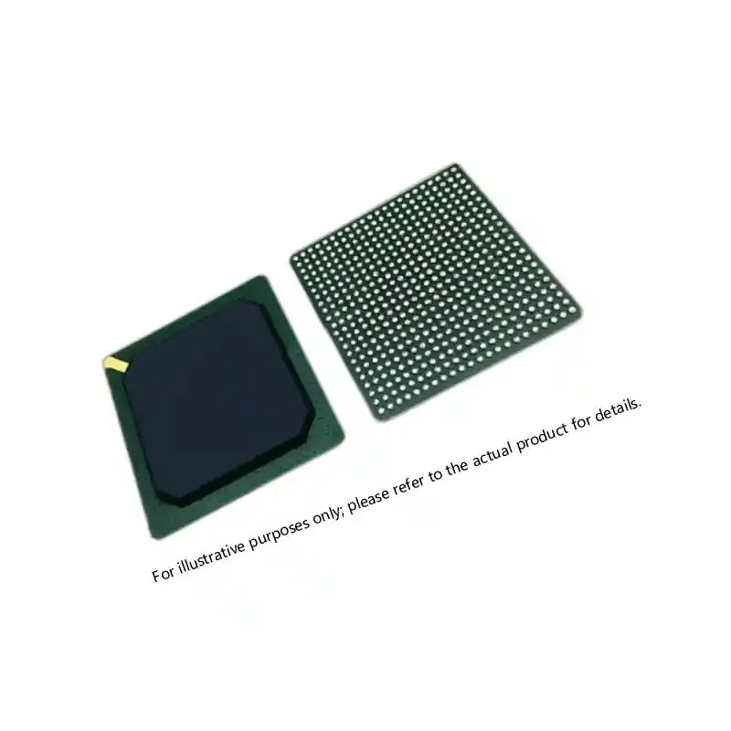
Signal integrity in military PCB design is often framed as a routing problem, but the first constraint is the parts themselves. High-speed ADCs and DACs with JESD204B or JESD204C interfaces force a specific lane count, data rate, and termination scheme. DDR memory devices add timing margins that cannot be repaired by trace length alone. When the design is qualified around a specific FPGA & CPLD family, the board pad pattern and pin-out are usually frozen at the same time as the stack-up and impedance targets.
Why Do Power and Ground Planes Decide Signal Integrity Before Routing Does?
Return current paths are set by the plane stack, not by the signal router. A split plane under a high-speed bus creates a discontinuity that no amount of trace tuning can remove. In our BOM reviews, we ask whether the plane arrangement can accept the final pin-out of each approved FPGA and data converter before the layout team starts routing. If a second-source part moves a high-speed lane to a different bank, the board may need a new plane arrangement, not a simple netlist change.
This is why pin-out compatibility is part of component selection. A drop-in replacement should mean drop-in at the electrical level, not only at the package outline.
What Documentation Should Defense Buyers Require Before Accepting a Board?
Documentation is where many military PCB design programs fail after the hardware works. The board itself may meet the electrical spec, but the acceptance package will be rejected if the paper trail is incomplete. Buyers should require bare board certification to IPC-6012 Class 3A or the applicable MIL-PRF-31032 or MIL-PRF-55110 requirement, along with material and plating certificates. For components, request lot traceability from the original manufacturer, screening method, and any C of C or QML documentation that ties the shipped part to the paperwork.
The same rule applies to changes. When a supplier proposes an alternate FPGA, memory device, or passive, compare the documentation package, not just the part number. A footprint match without the same qualification evidence does not protect the program during a customer or government audit.
That is the gap we work in. If the board build depends on 5962-series, JANTX, or QML devices, send the part list and required screen levels to xuansc2144@gmail.com. We will confirm availability, traceability, and lead time for each line before the layout is frozen, so the acceptance package arrives with the hardware instead of weeks behind it.
What Do Defense Buyers Ask About Military PCB Design and Component Sourcing?
Is IPC-6012 Class 3 enough for a military board?
No. IPC-6012 Class 3 covers fabrication and acceptance requirements, but a military program usually adds a performance specification such as MIL-PRF-31032 or MIL-PRF-55110, plus environmental and documentation requirements. The difference matters because a bare board can meet the IPC acceptance criteria and still lack the material controls, thermal stress screening, or traceability evidence the end customer expects. Treat IPC-6012 Class 3 as the baseline, not the ceiling.
Can commercial parts be used on a military PCB if they pass electrical testing?
That assumption fails because bench testing does not reproduce lot-level burn-in, temperature cycling, vibration, or the documentation trail behind MIL-STD-883 and QML devices. A part can pass a functional test today and still carry an unknown mixed lot history. Some programs allow upscreened commercial parts under defined limits, but that decision belongs to the program authority, not the assembly shop. The board layout must reflect the approved grade, not the hope that testing will close the gap.
Why do two QML parts with the same function behave differently on the same board?
It depends on the package, die revision, and process flow, not only the logic function. A ceramic column grid array and an organic BGA can have different CTE and solder joint fatigue behavior even when both meet QML documentation requirements. A die shrink or mask change can also alter electrical corners while the part number stays the same. That is why qualification evidence should be tied to the exact lot and package, not to a generic function description.
How early should component sourcing enter the PCB design process?
In programs we have worked, component sourcing enters too late when the first BOM reaches procurement after the layout is complete. The workable point is before placement. Once the approved part list, package mix, and qualification evidence are known, the stack-up, pad design, and plane assignments can be locked with fewer rework loops. If your next layout will mix QML and upscreened commercial devices, send the BOM and required screen levels to xuansc2144@gmail.com and we will confirm what evidence is available for each line.
If you’re interested, check out these related articles:
Virtex-7 690T FPGA: Performance, Packaging, and Reliability Insights
XC7VX485T FPGA: Virtex-7 Performance for Defense
Virtex-7 XC7VX690T: Performance and Reliability Insights
XCKU085 UltraScale FPGA: Performance for Critical Systems