Silicon Carbide (SiC) Power Semiconductors for Defense High-Power Systems
Table of Contents
- How SiC Improves Defense High-Power System Performance
- SiC Device Options for Military High-Power Stages
- What Qualification Standards Apply to SiC in Defense Systems
- Thermal Management and Integration Practicalities
- Sourcing SiC Semiconductors for Long-Duration Defense Programs
- Questions Defense Engineers Ask About SiC High-Power Semiconductors
Silicon carbide power semiconductors are reshaping how defense systems handle high voltages, fast switching, and extreme temperatures. For program managers and power supply engineers working on radar transmitters, directed-energy weapons, hybrid-electric combat vehicles, and shipboard power distribution, adopting SiC means improving efficiency, reducing cooling burden, and shrinking converter size. The challenge is that moving from silicon IGBT modules to SiC MOSFETs and diodes requires more than a datasheet comparison. You need components that meet military qualification standards, survive rugged environments, and stay available across a program’s decades-long lifecycle. Understanding where SiC outperforms silicon, what device options exist, and how to qualify and source these parts is the practical starting point for any defense high-power design.
How SiC Improves Defense High-Power System Performance
The advantage of silicon carbide over silicon in power conversion comes down to its wider bandgap. A silicon carbide MOSFET blocks higher voltage with the same die thickness, switches faster with lower energy loss, and operates at junction temperatures that would destroy a silicon IGBT. In a military pulsed-power application like an AESA radar transmitter, that translates to higher pulse repetition rates, smaller energy storage capacitors, and less thermal derating.
Defense systems benefit from SiC in three specific ways. First, switching losses at high frequency drop significantly when the output capacitance and gate charge of a SiC MOSFET are a fraction of a comparable silicon device. A 1,200 V SiC MOSFET can switch at 100 kHz or more, enabling the use of smaller magnetics and capacitors in a DC-DC converter for a vehicle-mounted power supply. Second, SiC Schottky diodes exhibit zero reverse recovery charge, eliminating the turn-on current spike that stresses silicon MOSFETs and raises EMI. In a high-voltage battery charger for a military ground vehicle, that reduces filtering requirements and heat sinking. Third, intrinsic carrier concentration in SiC stays low beyond 600°C, so leakage current remains manageable at operating temperatures where silicon devices fail. For directed-energy weapon capacitor banks that see repeated high-current pulses, that thermal margin means fewer forced-air or liquid-cooling loops inside an already dense chassis.
When we support defense programs transitioning from silicon IGBT bricks to SiC half-bridge modules, we see the design tradeoffs shift. For the same 10 kW output, a SiC-based LLC resonant converter can run at twice the frequency of its silicon predecessor, which cuts the transformer core volume roughly in half. That size and weight saving is not a datasheet talking point; it is a real SWaP-C improvement that affects how many power boxes fit in a vehicle bay or how much payload capacity remains on an airborne platform.
SiC Device Options for Military High-Power Stages
Selecting the right SiC component for a military power stage means matching the topology and voltage rail to the available device construction. The three primary building blocks are discrete MOSFETs, discrete Schottky diodes, and multi-chip power modules.
For voltage rails from 650 V to 1,700 V, discrete SiC MOSFETs in TO-247-4 or SMD packages offer the lowest on-resistance per die area. A 1,200 V, 25 mΩ SiC MOSFET switching at 50 kHz in a bridgeless totem-pole PFC can achieve efficiency above 99% without the heavy heat sink a silicon super-junction MOSFET demands. When the design calls for a boost or buck converter front-end, pairing that MOSFET with a 1,200 V SiC Schottky diode removes the reverse recovery loss that trips overcurrent protection and generates heat in the switching node.
Where power levels exceed 10 kW per channel, multi-chip power modules simplify the mechanical layout. A half-bridge module combining multiple SiC MOSFET dice and anti-parallel SiC Schottky diodes in a single ceramic-insulated package handles high-side and low-side switching with matched stray inductance between the DC link and the switch node. MIL-PRF-19500 and JANTX-equivalent screening are not common in commercial SiC modules yet, but we have seen programs run additional screening and burn-in on production lots to satisfy reliability review boards. The cost increases, but so does confidence that the module will hold off 1,200 V after repeated thermal cycles in a vehicle engine compartment.
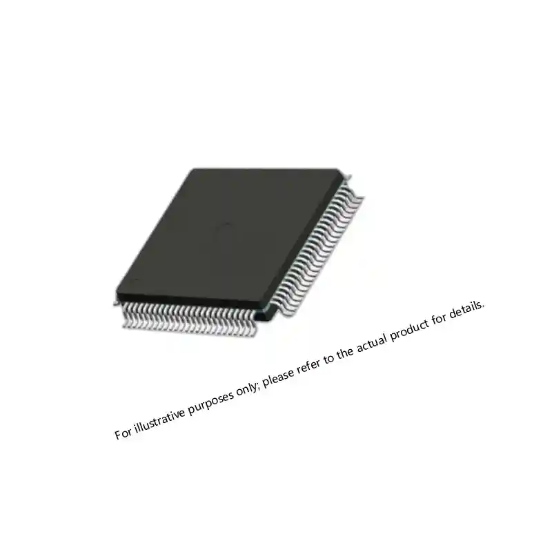
A practical point that often only surfaces during the BOM review is the gate drive voltage. Silicon IGBTs typically turn on with +15 V and block with –5 V to –15 V. SiC MOSFETs demand tighter gate voltage control. Under-driving a SiC gate increases R_DS(on) and switching loss; over-driving beyond the recommended +20 V limit degrades gate oxide reliability over time. We frequently see programs that spec the SiC devices correctly but overlook the gate driver IC until the bring-up phase, which delays qualification. Selecting an isolated gate driver with active Miller clamp and desaturation detection early avoids that rework.
If your program involves weapon system prime power or a high-altitude pulsed load, confirming the safe operating area under repetitive avalanche conditions before finalizing the BOM is worth an early conversation. Reach out at xuansc2144@gmail.com and we can check SiC device ruggedness data against your worst-case voltage excursion.
What Qualification Standards Apply to SiC in Defense Systems
The qualification baseline for military power semiconductors starts with MIL-PRF-19500 for discrete devices and extends to MIL-PRF-38534 for hybrid microcircuits that include power modules. Commercial SiC devices are typically tested to AEC-Q101 for automotive reliability, which provides useful data but does not replace the group A, B, and C testing required by MIL-PRF-19500.
Group A inspection covers static parameters at 25°C and over temperature. Group B adds mechanical and environmental tests: thermal shock, vibration, constant acceleration. Group C lifecycle testing includes high-temperature reverse bias and intermittent operating life, which are essential for SiC because the gate oxide interface trap density affects threshold voltage stability under prolonged high-temperature bias. A SiC MOSFET that passes 1,000 hours of high-temperature gate bias at 175°C ambient with less than 100 mV threshold shift is one you can trust in a power supply that must operate for 10,000 hours without maintenance. Without that data, you are extrapolating from short sample runs, and qualification authorities push back.
For custom SiC power modules, the path is different. A module that integrates MOSFET and diode dice on a DBC substrate falls under hybrid qualification. Burn-in at the module level at maximum rated junction temperature for 160 hours, per method 1015 of MIL-STD-883, is a common starting point. We have seen programs add 100 percent screening on module lots, including partial discharge test for isolation voltage, thermal impedance measurement using the body diode forward voltage method, and full dynamic characterization at rated current. These steps add cost and weeks of lead time, but they are the only way to generate the reliability data a defense program office will accept.
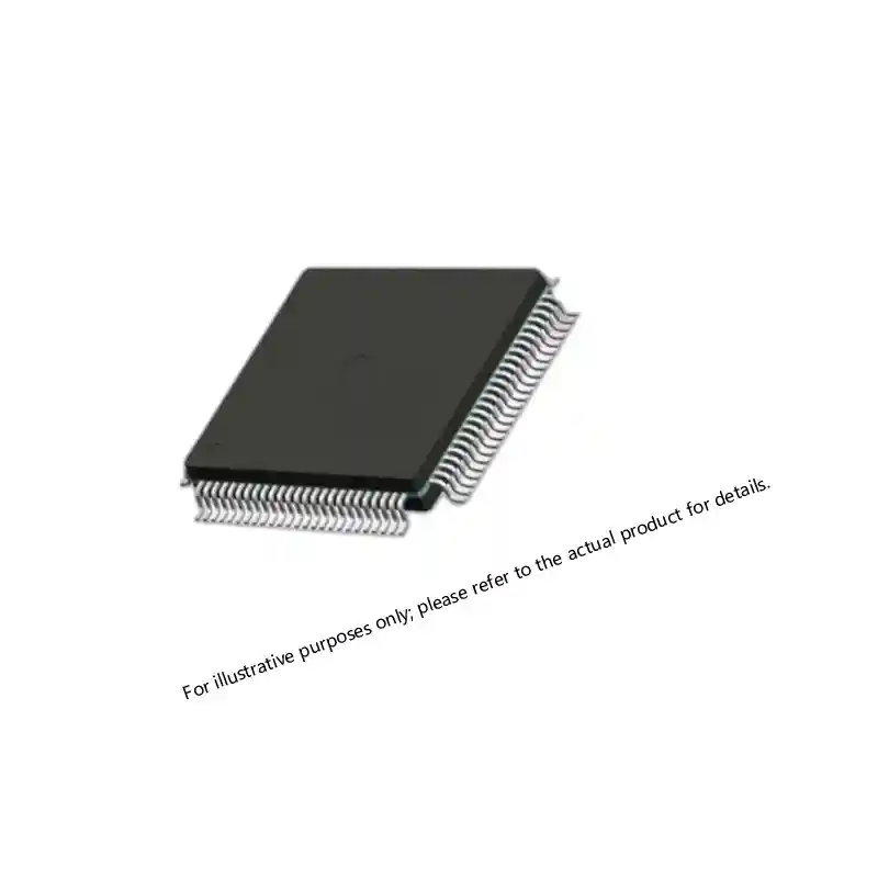
Packaging also influences how qualification data applies. Commercial SiC modules often use gel-filled plastic cases that are not hermetic. In a naval environment with salt fog exposure, moisture ingress through the case-to-baseplate interface can corrode bond wires over years. Defense programs operating in maritime or tropical conditions may require a hermetic metal-ceramic package, even if it increases thermal resistance slightly. When the sourcing decision is between a commercial-off-the-shelf module and a custom military package, the reliability difference often outweighs the upfront cost difference.
Thermal Management and Integration Practicalities
Even though SiC devices tolerate higher junction temperatures than silicon, the system still needs to remove heat. The difference is that with SiC you can allow a junction temperature of 175°C or 200°C instead of 125°C, which reduces the temperature delta required to move heat from the junction to ambient. In practical terms, a liquid-cooled cold plate running at 85°C inlet temperature can still cool a SiC module dissipating 300 W while keeping T_j below 175°C. A silicon IGBT module under the same boundary conditions would need colder coolant or a larger cold plate.
Thermal interface material selection matters more for SiC because the die area is smaller and heat flux density is higher. Sintered silver die attach and silicon nitride DBC substrates with direct bond copper layers minimize thermal resistance from junction to case. When we work with integrators transitioning to SiC power modules, the thermal stackup review often reveals that a legacy cold plate with thermal vias designed for a 30 mm × 30 mm IGBT footprint does not spread heat efficiently across the smaller SiC die array. A custom cold plate with copper inserts aligned to the SiC dice positions solves this, but it must be designed concurrently with the module layout, not as an afterthought.
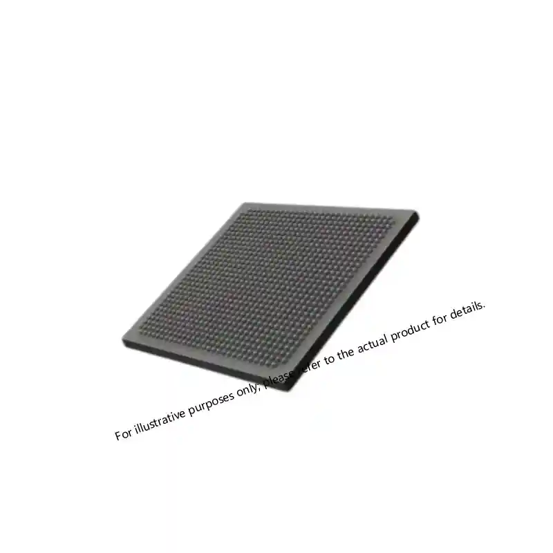
Parasitic inductance in the power loop is the other integration variable that bites designs that push switching frequency above 50 kHz. The DC link busbar layout between the input capacitors and the SiC half-bridge module must minimize the loop area to keep voltage overshoot under the device breakdown rating during turn-off. Laminated bus bars with overlapping positive and negative copper planes are the standard solution, and they become more important as current and dV/dt rise. Selecting a power module with Kelvin source connections for the gate drive loop further reduces common-source inductance that slows switching and increases loss.
Sourcing SiC Semiconductors for Long-Duration Defense Programs
Defense programs have supply chain requirements that commercial procurement does not. A SiC device that works electrically must also come with traceability documentation, a certificate of conformance, and confidence that the same part number will be available ten years from now when a mid-life upgrade is scheduled.
The SiC wafer supply is concentrated, and allocation decisions favor high-volume automotive and industrial customers first. A 1,200 V, 20 mΩ SiC MOSFET that is plentiful for an electric vehicle inverter may go on allocation when a defense program needs low hundreds of pieces per year. We maintain relationships with multiple SiC manufacturers and use our Aerospace & Defense category inventory to bridge gaps, but program offices benefit from placing rolling forecast orders that give wafer suppliers visibility into long-term demand. That forecast turns a spot-buy into a planned allocation, which stabilizes delivery and price.
Part number changes and die revisions also affect defense programs more than commercial ones. A SiC MOSFET datasheet may change the R_DS(on) specification by 5 percent between die revisions, which is fine for a commercial power supply but may trigger a requalification in a military design. We advise customers to lock in a specific lot or wafer fab process revision and procure enough inventory to cover production, prototyping, and spares for the program phase. Die banking for custom modules is another strategy; purchasing known-good die and storing them in a controlled nitrogen atmosphere extends availability beyond the commercial product lifecycle.
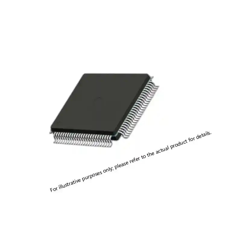
Documentation is as critical as the component itself. A certificate of conformance for a SiC MOSFET should reference the manufacturer’s lot number, the test standards used, and the observed parametric data. For programs requiring full lot-test reports, we coordinate with the SiC manufacturer or an approved test house to run the required group A, B, and C inspections and deliver the data package with the shipment. Without that paperwork, incoming inspection at the defense contractor’s facility will quarantine the parts, and the program schedule suffers.
Questions Defense Engineers Ask About SiC High-Power Semiconductors
What is the primary reliability concern with SiC MOSFETs in military power supplies?
Gate oxide integrity under long-term high-temperature bias. Threshold voltage drift over time can lead to parametric shifts that affect converter performance. Screening to 1,000 hours at maximum rated gate voltage and temperature, with strict delta-V_th limits, mitigates this.
Can we use commercial automotive-grade SiC modules in a ground vehicle power system?
Physically yes, but qualification documentation will be lacking. AEC-Q101 data is a starting point; you still need the additional group B and C tests per MIL-PRF-19500 or program-specific requirements. Without those, the reliability review board may not approve the part.
Is hermetic packaging required for SiC in naval applications?
If the module will be exposed to high humidity and salt fog without a sealed enclosure, hermetic packaging reduces moisture-related failure risk. In practice, many shipboard converters use sealed cabinets with controlled humidity, so non-hermetic modules with conformal coating can work if the environment is managed.
How do we handle the higher dV/dt of SiC when retrofitting a silicon IGBT design?
The faster switching edge increases common-mode EMI and reflected wave voltage spikes. You need to add common-mode chokes on the input and output, use shielded cables with shorter runs, and possibly add a snubber at the motor terminals if driving a motor load. Start with a detailed EMI pre-compliance scan early.
What documentation do we need to accept a SiC lot for a MIL-PRF-19500 compliant program?
At minimum, the certificate of conformance with lot number and test data traceable to the manufacturer’s quality system. For flight-critical or safety-critical applications, full lot-test reports covering group A, B, and C parameters are standard. We can arrange lot-specific testing through approved labs when the manufacturer’s standard documentation does not meet program requirements. Share your program’s data package requirements with us at xuansc2144@gmail.com and we will confirm what testing and paperwork can be provided before shipment.
If you’re interested, check out these related articles:
Virtex-7 690T FPGA: Performance, Packaging, and Reliability Insights
XC7VX485T Virtex-7 FPGA: Performance and Sourcing for Defense
Virtex-7 690T FPGA: Performance for Mission-Critical Systems