
TPS7A8500ARGRR 3A Low-Noise LDO: QFN-20 Sourcing Guide
Table of Contents
- Typical Electrical Characteristics
- Layout and Thermal Design Rules
- Low-Noise Design for RF and Data Conversion
- Screening, Traceability, and Documentation
- Sourcing and Compliance Checklist
- Companion Components for FPGA Power Trees
- Documented RFQ Support
- Sourcing TPS7A8500ARGRR Through Sparkle Electronics
- Frequently Asked Questions
- Is the TPS7A8500ARGRR a qualified MIL-SPEC part?
- What output voltages are supported?
- What are the main benefits for RF and data converter applications?
- How should the exposed pad be handled during reflow?
- What documentation should I request before buying?
- References
Power-supply noise is among the most consequential variables in high dynamic range signal chains. In radar processors, electronic warfare receivers, and software-defined radio platforms, a noisy voltage rail degrades ADC spurious-free dynamic range, increases FPGA transceiver jitter, and can make calibration results unstable. The TPS7A8500ARGRR addresses this with 3 A output capability, low output noise, and an adjustable 0.8 V to 5.2 V output range in a compact QFN-20 package. For defense electronics teams, the part offers a practical bridge between high-efficiency switching converters and sensitive analog or digital loads.
Typical Electrical Characteristics
The values below are manufacturer-published typical values and should be verified against the latest datasheet before design freeze.
| Parameter | Typical Value | Design Impact |
|---|---|---|
| Output voltage range | 0.8 V to 5.2 V, adjustable | Covers ADC/DAC analog rails, FPGA transceiver rails, and low-voltage DSP cores |
| Output current | 3 A continuous | Supports multiple point-of-load rails when thermal design is adequate |
| IN voltage range | 1.1 V to 6.5 V | Works from low-voltage intermediate rails |
| BIAS voltage range | 3.0 V to 6.5 V | Separate bias pin improves dropout and PSRR |
| Output noise | ~4.4 µV RMS, 10 Hz–100 kHz | Preserves SNR and SFDR in data converters |
| PSRR | High PSRR beyond 1 MHz | Rejects switching ripple from upstream DC-DC stages |
| Package | QFN-20 with exposed thermal pad | Small footprint supports SWaP-C constrained boards |
The ARGRR suffix identifies the adjustable-output version with QFN-20 packaging and tape-and-reel supply. When locking a bill of materials, confirm that the suffix exactly matches the intended packing and screening path.
Layout and Thermal Design Rules
The QFN-20 package depends on a soldered exposed pad for thermal performance. Place the pad on a continuous ground plane and use an array of thermal vias to pull heat into inner copper layers. Without adequate copper, the 3 A rating is not achievable at high ambient temperature.
Decoupling belongs close to the device. Keep the IN and BIAS loop areas small, and place the input capacitors between the pins and ground with minimal trace length. Route the feedback divider as a quiet trace, away from switching nodes and high dI/dt paths. If the design uses remote sense or a separate output sense connection, route that trace as a Kelvin connection to avoid voltage error at the load.
Output capacitance should follow the datasheet recommendation, with particular attention to effective capacitance after DC bias derating. Low-ESR ceramic capacitors are common, but stability margins can shift if the output impedance profile is outside the intended range.
Low-Noise Design for RF and Data Conversion
The TPS7A8500ARGRR is most valuable when it post-regulates a switching converter output. The preceding DC-DC stage provides efficiency; the LDO removes high-frequency ripple and supply ringing before the rail reaches sensitive circuits.
For high-speed ADCs, DACs, and PLLs, the low output noise of this part helps protect signal-to-noise ratio and clock phase noise. Keep noisy digital return currents away from the analog ground pour, and place the LDO as close as possible to the load. A series ferrite bead between the switching stage and LDO can add attenuation, but the bead should be damped to avoid creating a resonant peak at the LDO input. The LDO’s PSRR does the heavy lifting above a few hundred kilohertz; the bead is a supplement, not a substitute for proper layout.
When powering FPGA transceiver rails, account for start-up sequencing and inrush current. The adjustable output range supports common 1.0 V, 1.8 V, 2.5 V, and 3.3 V rails. Programmable soft start, where available in the final configuration, reduces current spikes and simplifies sequencing with adjacent regulators.
Screening, Traceability, and Documentation
For defense and aerospace programs, component qualification is a supply-chain decision as much as a design decision. Many TPS7A8500ARGRR applications are built around commercial or industrial-grade material that is then subjected to documented upscreening. Screening plans commonly include external visual, temperature cycling, and burn-in methods selected from MIL-STD-883K [1]. When a program requires QML Class Q or Class V devices, procurement must follow MIL-PRF-38535 [2]; this commercial-grade LDO variant may require a suitability review before being placed on an approved vendor list for qualified builds.
Electrostatic discharge control is required during incoming inspection, kitting, and assembly. ESD-protected workstations should follow ANSI/ESD S20.20 [3]. Board-level reliability validation can include temperature cycling per JEDEC JESD22-A104 [4]. Moisture/reflow sensitivity for the nonhermetic QFN package should follow IPC/JEDEC J-STD-020 classification practices [5].
Counterfeit risk is a central concern when sourcing parts outside authorized channels. Before accepting material, verify date and lot codes, manufacturer markings, and reel labels. A credible C of C, lot traceability documentation, and incoming electrical sampling are the minimum controls for defense electronics receiving inspection. Components with erased or blacktopped markings should be quarantined immediately.
Sourcing and Compliance Checklist
Before purchasing TPS7A8500ARGRR for a military or high-reliability design, confirm the following:
- Exact part number and packing suffix, including any screening or temperature grade
- Full manufacturer lot and date code documentation
- Required screening level and whether upscreening is acceptable
- ESD, MSL, and dry-pack handling records
- Certificate of Conformance and lot test data, where required
- Incoming electrical sample plan for output voltage accuracy and noise
- Export-control and DFARS compliance review for the final assembly
Companion Components for FPGA Power Trees
The TPS7A8500ARGRR frequently appears in power trees for high-density FPGAs used in radar processing, SIGINT, and secure communications. Sparkle Electronics maintains representative inventory of complementary FPGA devices for integrated supply planning:
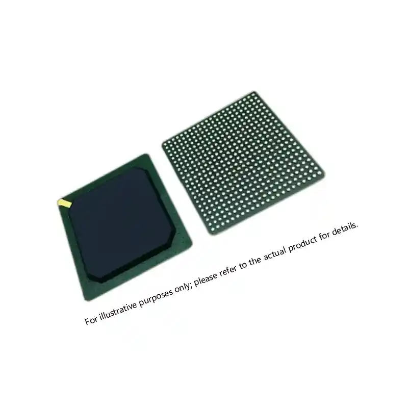
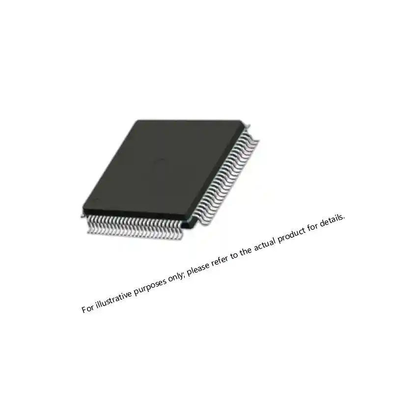
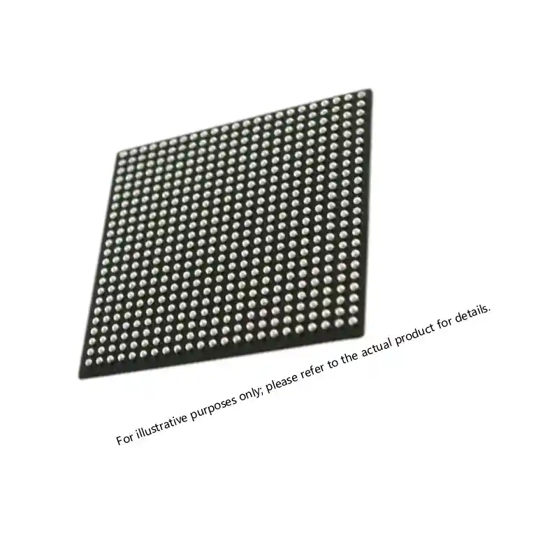
Evaluating the full power tree is as important as selecting the LDO itself. > When TPS7A8500ARGRR is used for FPGA transceiver and core rails, engineers usually validate the full power tree; <XCKU085 UltraScale FPGA: Performance for Critical Systems> covers FPGA selection, performance, and supply planning.
Documented RFQ Support
For BOM-level quotes or screening coordination, Sparkle Electronics supports defense and research procurement teams. Send the part number, target quantity, delivery date, and any QML or upscreening requirement to xuansc2144@gmail.com. Inquiries are routed to the same supply-chain team that manages documentation, lot traceability, and incoming verification.
Sourcing TPS7A8500ARGRR Through Sparkle Electronics
Sparkle Electronics is a specialized distributor of military-grade and high-reliability electronic components, serving defense contractors, systems integrators, and research institutions in more than 30 countries. The company supports TPS7A8500ARGRR and related low-noise power components with documentation review, screening coordination, and long-term program supply planning.
For pricing, availability, or a BOM-level quotation, contact Sparkle Electronics at xuansc2144@gmail.com. To help the team respond quickly, include the part number, required quantity, target delivery date, screening or QML requirements, and destination country for export-compliance review. The company’s focus is not transactional part supply alone; it is maintaining the documentation, traceability, and repeatable inspection discipline that defense procurement teams require.
Frequently Asked Questions
Is the TPS7A8500ARGRR a qualified MIL-SPEC part?
The TPS7A8500ARGRR is a high-performance commercial or industrial-grade LDO. It is not a substitute for a QML Class Q or Class V device unless the program accepts documented upscreening. Always confirm the required qualification path before placing it on a defense approved vendor list.
What output voltages are supported?
The output is adjustable from 0.8 V to 5.2 V using an external resistor divider. This range covers common analog, digital, and transceiver rails in signal-chain designs.
What are the main benefits for RF and data converter applications?
Low output noise and high PSRR help preserve SNR, SFDR, and clock phase noise. The 3 A output current also supports multiple mixed-signal loads from one compact QFN-20 footprint.
How should the exposed pad be handled during reflow?
The exposed pad must be soldered to the ground plane for thermal and electrical performance. Use a stencil-matched solder volume and thermal vias, and follow the moisture and reflow classification practices in IPC/JEDEC J-STD-020 [5].
What documentation should I request before buying?
Request the manufacturer lot and date code, C of C, ESD and dry-pack records, and incoming electrical test data. For qualified defense builds, also confirm the screening plan and traceability package.
References
[1] U.S. Department of Defense. MIL-STD-883K, Test Method Standard for Microcircuits. 2018.
[2] U.S. Department of Defense. MIL-PRF-38535J, Performance Specification: Integrated Circuits (Microcircuits) Manufacturing, General Specification for. 2010.
[3] ANSI/ESD S20.20-2021. Protection of Electrical and Electronic Parts, Assemblies and Equipment. 2021.
[4] JEDEC. JESD22-A104, Temperature Cycling. 2020.
[5] IPC/JEDEC. J-STD-020, Moisture/Reflow Sensitivity Classification for Nonhermetic Solid State Surface-Mount Devices. 2021.
If you’re interested, check out these related articles:
Virtex-7 XC7VX690T: Performance and Reliability Insights
XCKU115 UltraScale FPGA: Powering Critical Defense Systems
Virtex-7 XC7VX690T: Performance, Reliability, and Integration