Military-Grade FPGA Programming: Tools and Best Practices for Defense
Table of Contents
- The FPGA Programming Environment in Defense Systems
- Choosing FPGA Families That Meet Defense Requirements
- Best Practices for Military FPGA Design and Implementation
- Securing FPGA Bitstreams and Configuration
- Managing Supply Chain and Qualification for FPGA Programs
- Common Concerns When Programming Military FPGAs
- How does QML-Q differ from QML-V for FPGAs?
- Can commercial FPGA development tools be used for military designs?
- How do we handle obsolescence when a legacy military FPGA must be reprogrammed?
- Is a flash-based FPGA inherently immune to radiation-induced upset?
- What documentation does a defense program require for FPGA design sign-off?
Programming military-grade FPGAs extends well beyond writing VHDL or Verilog. It requires selecting device families that meet QML qualification levels, securing configuration bitstreams against tampering, and ensuring long-term supply for programs that can span decades. For defense systems, the programming workflow runs from architecture definition through bitstream generation to in-field update management, all under strict documentation and traceability. This article provides best practices and tool insights drawn from over twelve years of defense electronics procurement and support, giving design teams a practical roadmap for mission-critical FPGA programming.
The FPGA Programming Environment in Defense Systems
Defense FPGA development relies on vendor-specific toolchains that directly support military-grade device families. Xilinx Vivado handles Virtex-7, Kintex-7, and Spartan-6 parts. Microchip Libero SoC covers SmartFusion2, IGLOO2, and PolarFire devices. Intel Quartus Prime Pro supports Stratix 10 and Cyclone 10 GX families. Each toolchain provides synthesis, place-and-route, timing analysis, and bitstream generation, but the critical difference for defense programs is the availability of device models that account for extended temperature ranges and radiation effects.
Timing closure becomes significantly tighter when the operating range spans minus 55 degrees Celsius to 125 degrees Celsius. Setup and hold margins that pass at room temperature can fail at the cold corner on a fast process corner die, so static timing analysis must use military-grade speed files and appropriate derating factors. I have seen designs that passed commercial timing but required three respins to meet defense timing, simply because the initial constraints assumed industrial temperature margins.
Many tool versions also support encrypted netlist flows and secure configuration modes required by defense programs. If you use an older tool version that lacks these features, the only path forward is an upgrade or a waiver, and waivers are not granted lightly.
| FPGA Family | Technology | Typical Defense Use | Primary Tool |
|---|---|---|---|
| Xilinx Virtex-7 | SRAM | Radar, EW, SIGINT | Vivado |
| Microchip SmartFusion2 | Flash | Avionics, secure comms | Libero SoC |
| Actel Axcelerator | Antifuse | Missile guidance, space | Libero IDE |
| Intel Stratix 10 | SRAM | High-performance computing | Quartus Prime Pro |
| Xilinx Kintex-7 | SRAM | UAV payloads, SDR | Vivado |
Choosing FPGA Families That Meet Defense Requirements
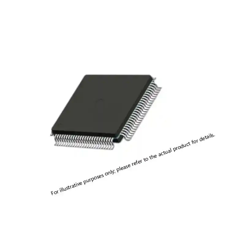
Three underlying technologies dominate military FPGAs. SRAM-based devices from Xilinx and Intel offer the highest logic density and DSP resources but require an external configuration memory and a secure boot process. Flash-based FPGAs from Microchip, including ProASIC3 and SmartFusion2, store configuration on-chip, so they are live at power-up and inherently resistant to configuration memory upset. Antifuse parts like the Actel Axcelerator family are one-time programmable and immune to radiation-induced configuration corruption, making them standard in missile and space applications.
The selection of the FPGA family directly shapes the programming workflow. An SRAM FPGA needs a secure bitstream loading sequence, often requiring a separate CPLD or microcontroller to manage authentication and decryption. A flash FPGA simplifies this but may limit logic density. If the design requires both high gate count and single-event upset immunity at the configuration level, you must consider mitigation strategies such as scrubbing, not just part selection.
For programs that already have approved vendor lists, cross-referencing the required 5962 or QML part numbers against available speed grades and packages early prevents delays. I have supported programs where a preferred Virtex-5 part was discontinued before prototyping was complete, forcing an emergency redesign around a different package. A simple QML database check at the start would have flagged the issue. If your design involves a mix of high-density logic and flash security, the best approach is to evaluate both technology paths against your documentation and long-term supply constraints. Share your BOM requirements with us and we can help identify a family that avoids single-source risk.
Best Practices for Military FPGA Design and Implementation
Start with a formal design specification that defines functional requirements, interface standards, and environmental constraints. For FPGA programming, this specification must also define the target device, package, speed grade, and configuration memory type. Without this, the design team can drift toward a convenient commercial part that later fails qualification.
Use hierarchical design partitioning that separates mission-critical functions from non-critical logic, making it easier to apply different verification depths. For timing-critical paths, manually constrain clocks and input/output delays rather than relying on automatic constraint generation. Defense designs often involve multiple clock domains, and crossing them without proper synchronization creates intermittent failures that surface only under extreme conditions. I have resolved field failures where a missing double-flop synchronizer passed bench testing but failed at minus 40 degrees.
Version control and traceability are not optional in defense programs. Every synthesis run, every constraint change, and every bitstream must be linked to a design revision and archived. Regulated programs require traceability from requirements to test results, and a well-structured FPGA development environment makes audits straightforward rather than painful.
Simulate with post-layout timing models and include corner-case testing across voltage and temperature. Prototype on actual silicon even when the schedule is tight, because behavioral simulation alone misses I/O edge rate and power-on reset behavior that can differ from the model.
Securing FPGA Bitstreams and Configuration
For SRAM-based FPGAs, bitstream security begins with AES-256 encryption and key storage in battery-backed or eFuse memory. The configuration process must authenticate the bitstream before loading, using HMAC or similar methods to detect tampering. After configuration, disable readback capability and, where the device supports it, enable bitstream verification to confirm the loaded image matches the intended one.
Flash-based FPGAs simplify configuration security because the bitstream never leaves the device, but the design must still protect against unauthorized readback through JTAG or SPI interfaces. Use permanent lock bits and, in SmartFusion2 and PolarFire devices, the user security features that prevent memory extraction.
A practical step often overlooked: the configuration memory itself must be sourced with the same traceability as the FPGA. If you are using a Xilinx Platform Flash or a serial NOR device, verify that the memory part also meets the program’s temperature range and has a valid Certificate of Conformance. I have seen a configuration memory failure ground an entire fleet’s firmware update, which took weeks to resolve because the memory part was not on the approved component list.
Managing Supply Chain and Qualification for FPGA Programs
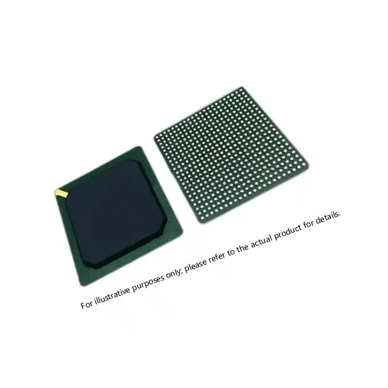
The FPGA you select today must remain producible and compliant for the life of the program, which can be twenty years or more. Even with active parts, certain speed grades and package options are discontinued without fanfare. Designers who program military FPGAs must validate the full part number, including temperature range, package, and speed grade, against the latest QML and Qualified Parts List before freezing the design. The Defense Logistics Agency QML database and the manufacturer’s product change notifications are the authoritative sources, not distributor stock status.
Long-term supply planning also includes configuration memory, programming cables, and any support components that are part of the programming chain. A last-time buy for the FPGA means nothing if the configuration PROM becomes unavailable two years later. Second-source strategies, die banking, and cooperative agreements with distributors who understand defense program timelines become essential.
At Sparkle Electronics, we specialize in sourcing military-grade FPGAs from Xilinx, Microchip, Intel, and others, with full traceability and QML documentation. Whether you are planning a new design or facing an end-of-life notice on a legacy FPGA, email your BOM to xuansc2144@gmail.com and we will help you find a sustainable path forward that meets the compliance requirements of your program.
Common Concerns When Programming Military FPGAs
How does QML-Q differ from QML-V for FPGAs?
QML-Q is the baseline military qualification under MIL-PRF-38535, requiring the manufacturer to demonstrate a controlled process, screening per method 5004, and ongoing quality conformance inspection. QML-V adds tighter requirements for radiation hardness assurance and is typically assigned to devices intended for space and strategic systems. For most ground-based and avionics applications, QML-Q is sufficient, but if your program operates in a high-radiation environment, specify QML-V parts and verify the radiation test reports, not just the label.
Can commercial FPGA development tools be used for military designs?
Yes, the same Vivado, Libero, or Quartus tools are used for both commercial and military devices. The tool itself does not differentiate. What matters is that you select the correct device family, use military temperature-grade timing models, and apply the security and verification flows required by your program. Some older military FPGAs may require legacy tool versions, so maintaining a tool archive is a supply chain consideration in itself.
How do we handle obsolescence when a legacy military FPGA must be reprogrammed?
Start by contacting the manufacturer to confirm the last-time buy status and check if a pin-compatible replacement exists. If the original programming files are from an older tool version, you may need to migrate the design to a current tool version, which can involve re-synthesis and re-verification. In parallel, identify second-source options or plan a technology refresh that targets a currently qualified FPGA family. The redesign effort should include a configuration memory update.
Is a flash-based FPGA inherently immune to radiation-induced upset?
Not entirely. Flash-based FPGAs are immune to configuration memory upset because the configuration cell is a non-volatile transistor. However, the user logic flip-flops and block RAM are still susceptible to single-event upsets, so mitigation techniques such as triple modular redundancy and error-correcting codes are still required for critical functions.
What documentation does a defense program require for FPGA design sign-off?
Typically, a design description document, a verification plan with test results, a traceability matrix linking requirements to test cases, and a configuration management plan that describes bitstream versioning and storage. For programs under formal configuration control, the FPGA design package must also include evidence that the programming files were generated from the controlled source code and have not been modified post-build. If you are preparing for a review and need to source qualified FPGAs with the right documentation, send your part numbers and qualification requirements to xuansc2144@gmail.com and we will confirm availability and traceability before you commit.
If you’re interested, check out these related articles:
XC7VX485T Virtex-7 FPGA: Performance and Sourcing for Defense
Virtex-7 690T FPGA: Performance for Mission-Critical Systems
UltraScale KU085 FPGA Specifications for Defense Systems
XC7VX485T FPGA: Virtex-7 Performance for Defense