Microsemi Military FPGAs: ProASIC and SmartFusion Sourcing
Table of Contents
- How ProASIC and SmartFusion Differ in Defense Systems
- ProASIC Series: Instant-On, Non-Volatile FPGAs for Mission-Logic
- SmartFusion Series: Integrated ARM Cortex-M3 SoC for Processing-Centric Designs
- Sourcing Strategies for Microsemi Military FPGAs
- Compliance and Traceability Requirements
- Key Considerations for Engineers and Procurement Teams
When a defense program requires an FPGA that powers up instantly, tolerates radiation without configuration loss, and meets QML qualification, the choice frequently narrows to the ProASIC and SmartFusion families from Microsemi (now part of Microchip). These non-volatile, flash-based military FPGAs deliver design security and single-event upset immunity that SRAM-based alternatives cannot match without external configuration storage, but beyond the datasheet performance, program managers must navigate lead times, part number transitions across the acquisition, and the documentation chain required for MIL-STD-883 compliance. Getting a reliable supply of authentic parts with full traceability is as critical as selecting the right logic density or feature set, and the sourcing strategy you adopt early can determine whether a prototype stays on schedule or stalls for months.
How ProASIC and SmartFusion Differ in Defense Systems
ProASIC and SmartFusion share the same flash-based, reprogrammable non-volatile foundation, but they target different system architectures. The differentiation comes down to whether your design needs an integrated processor subsystem or a pure, low-power logic fabric with instant-on capability.
ProASIC devices are logic-centric. The ProASIC3, ProASIC3E, and low-power ProASIC3L families scale from 60 k to 3 million system gates, all single-chip, live-at-power-up operation with no external boot memory required. The flash cells hold the configuration through power cycles and are inherently immune to configuration SEUs, which eliminates the scrubbing and configuration upset handling that SRAM-based FPGAs demand in radiation environments. This makes ProASIC a natural fit for control-plane functions, interface bridging, encryption engines, and other deterministic logic where a processor is unnecessary.
SmartFusion2 and the earlier SmartFusion add a hard ARM Cortex-M3 processor, dedicated flash for code storage, and configurable analog blocks alongside the FPGA fabric. The processor is clocked up to 166 MHz and has its own tightly coupled memory, so you can run real-time software without consuming logic resources for a soft CPU. The analog subsystem includes ADC, DAC, and comparators that connect directly to the FPGA routing, eliminating external mixed-signal components and their associated reliability points. In a defense context, SmartFusion2 supports secure boot, tamper detection, and encrypted program storage, making it suitable for systems that combine processing, monitoring, and sensor interfaces on a single die while maintaining security throughout the power cycle.
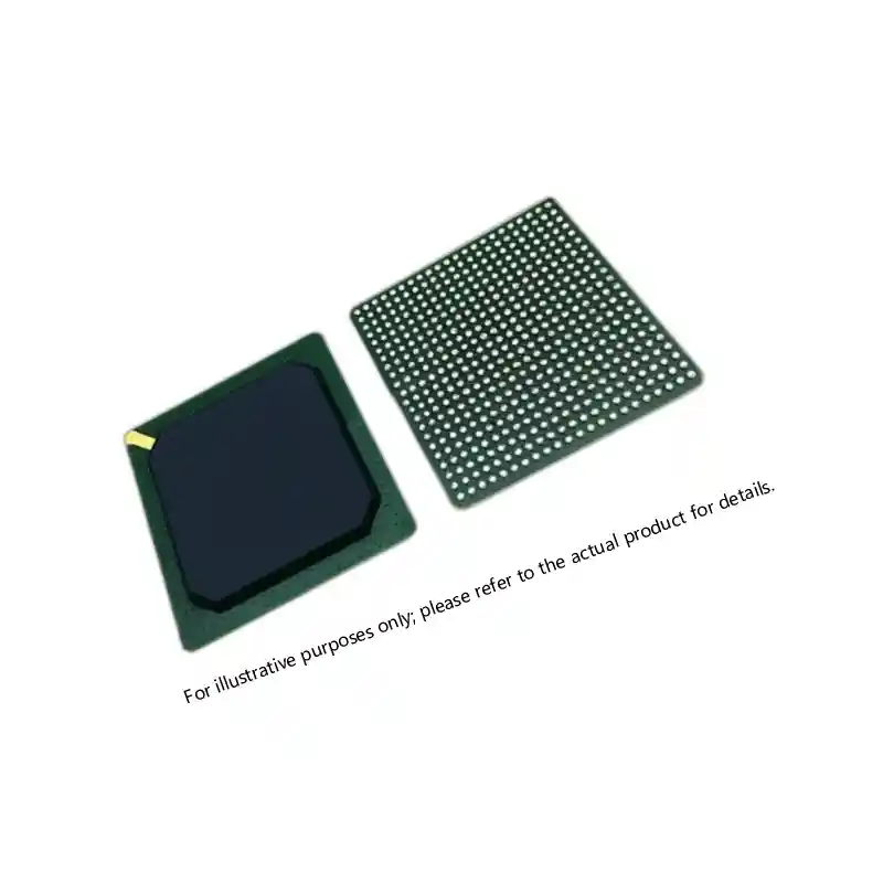
The table below summarizes the key architectural differences as they impact defense selection.
| Feature | ProASIC3/E/L | SmartFusion2 |
|---|---|---|
| Technology | Flash-based non-volatile FPGA | Flash-based SoC with hard ARM Cortex-M3 |
| Processor | None (instant-on logic only) | 166 MHz ARM Cortex-M3, dedicated flash |
| Logic capacity | 60 k – 3 M system gates | 5 k – 150 k logic elements + math blocks |
| Analog blocks | None | 12-bit ADC, DAC, comparators, temp sensor |
| Security | AES-128 bitstream encryption, FlashLock | AES-256, secure boot, tamper detection, zeroization |
| Package range | VQ100 to FG896, small footprint options | FG484 to FCG1152, high I/O count |
| Power (typ.) | Static current as low as 5 mA (ProASIC3L) | Active power optimized with multiple supply rails |
If your architecture is logic-heavy and you need to minimize bill-of-materials risk, ProASIC stays simpler. If you are consolidating a microcontroller, FPGA, and analog front-end, SmartFusion2 reduces board space and procurement complexity. I have seen programs where a decision to replace a separate CPLD and processor with a single SmartFusion2 cut the BOM line items by over 30%, which directly simplifies supply chain management.
ProASIC Series: Instant-On, Non-Volatile FPGAs for Mission-Logic
The appeal of ProASIC in defense electronics is not one feature but the combination of instant-on behavior, radiation tolerance of the configuration memory, and the absence of supply-chain dependencies on separate configuration devices. For missile control surfaces, fuze logic, power-on reset sequencing, or any application where the FPGA must be operational within microseconds of rail stabilization, ProASIC eliminates the boot window entirely.
Reprogrammability is an underappreciated advantage. Flash cells can be cycled thousands of times in-system, which means you can update logic without touching board-level hardware. This support for field upgrades without the risk of a corrupted bitstream during reconfiguration—because the device does not lose its existing function until the new image is validated—is a safety mechanism that matters when equipment is deployed and cannot return to a depot.
The military-temperature ProASIC3 and ProASIC3E parts are rated for -55°C to +125°C, with QML Class Q and Class V flows available. Part numbers like A3P1000-FGG484I or A3PE3000L-1FGG896I appear on approved vendor lists across multiple prime contractor programs, and we have supported BOMs that require specific speed grades and package variants across these families. One persistent challenge is that a given density point may be available in commercial, industrial, and military grades, but the military-tested version can carry a lead time extension of 8–16 weeks depending on wafer lot scheduling, so locking in the correct order code early—and confirming that the part is still in active production—prevents design cycle delays.
From a reliability perspective, the flash-based configuration cells eliminate the single-event functional interrupt (SEFI) and multiple-bit upset (MBU) risks that affect SRAM FPGAs in high-altitude and space-adjacent environments. There is no configuration scrubbing circuitry to design, validate, or maintain over the life of the program.
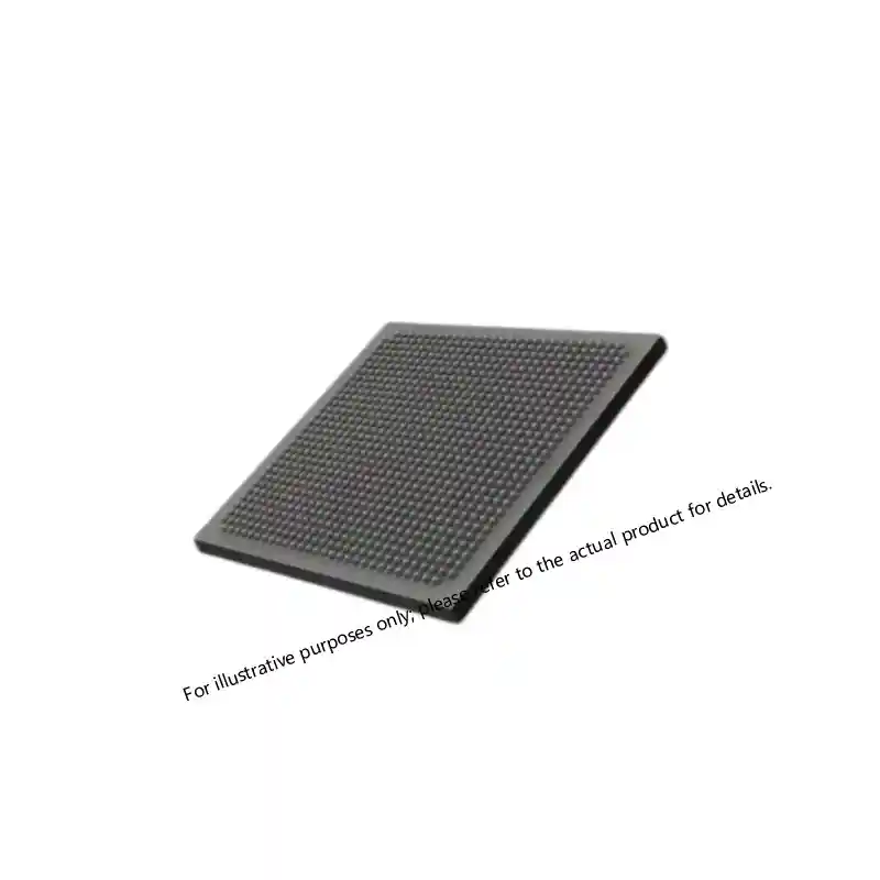
SmartFusion Series: Integrated ARM Cortex-M3 SoC for Processing-Centric Designs
When a defense subsystem needs to run a control loop, communicate over a serial bus, and monitor analog telemetry, the default approach has historically been a small microcontroller plus a separate FPGA, with the inevitable level-translation, timing closure, and obsolescence risk tied to two distinct part numbers. SmartFusion2 collapses that architecture into one device with deterministic, known interconnect timing.
The hard processor is not a soft core using FPGA resources. It has its own instruction and data caches, dedicated memory controllers, and a standard ARM debug interface, so you can develop and verify firmware independently of the FPGA design. We have seen this separation accelerate bring-up in programs where the software and FPGA teams work in parallel because the processor is a known quantity and does not depend on FPGA timing closure to start executing code.
The analog capability is not a token ADC channel. The SmartFusion2 devices include multiple 12-bit ADC inputs, a temperature monitor, and voltage comparators that can be routed internally so that over-temperature or undervoltage conditions trigger an FPGA response without external sensor components. For avionics or vehicle electronics where weight and board area are at a premium, removing even a handful of discrete analog components improves mean-time-between-failure numbers.
In programs that require cryptographic protection of the FPGA bitstream as well as the processor code, SmartFusion2 provides a hardware security block that enforces authenticated boot, encrypted external memory interfaces, and zeroization of internal flash on tamper detection. These features align with Common Criteria and FIPS 140-2 requirements, which increasingly appear as must-haves in secure communications and cryptographic ignition systems.
Sourcing Strategies for Microsemi Military FPGAs
The supply dynamics for Microsemi military FPGAs changed meaningfully after Microchip acquired the product lines. Part numbers migrated to a new numbering scheme, factory allocations were rebalanced, and several older ProASIC and SmartFusion die entered a “mature” status where new wafer starts are not guaranteed. A BOM that was stable for five years can suddenly face a 26-week lead time because the device is now planned only on a build-to-forecast basis.
For any program with a production horizon beyond 2028, you should verify whether the specific density and package combination is still in the active portfolio. If it has moved to mature, start the last-time buy conversation early. We have worked with programs that placed an LTB order two years before the final production run, and they avoided the panic that comes when a critical part is discontinued with no alternative. In some cases, die banking is available for particularly high-volume programs, where a wafer lot is reserved and bonded-out packages are drawn as needed.
The transition from Microsemi to Microchip also introduced some confusion in cross-referencing. A Microsemi part number like A2F500M3G-FGG484I became a Microchip part number in certain ordering systems, but the physical device is identical. However, some procurement systems reject the old number or flag it as end-of-life, causing false alarms. We recommend maintaining both the legacy and the new Microchip order code in your internal systems and confirming with the distributor which part number the factory currently recognizes for order entry.
Distribution channel matters. Authorized military component distributors have direct access to factory inventory and can provide the certificate of conformance and lot traceability that independent brokers often cannot match. When a defense contractor needs 50 pieces of A3PE3000L-1FGG896I with a full C of C and QML documentation, the sourcing path should be clear, documented, and repeatable.
If your program involves a mix of ProASIC for logic and SmartFusion for processing, bundling procurement through one competent distributor often reduces the overhead of managing multiple supplier quality audits and streamlines the incoming inspection process. At Sparkle Electronics, we regularly consolidate BOMs for defense clients and provide a single documentation package for all Microsemi line items, which simplifies both the receiving process and the auditor’s review.
Compliance and Traceability Requirements
Every military-grade Microsemi FPGA procured for a U.S. or allied defense program must be backed by documentation that proves authenticity and qualification status. The minimum expectation is a certificate of conformance that states the device meets the applicable MIL-PRF-38535 slash sheet, with a lot date code and an unbroken chain of custody from the factory through distribution.
For QML Class Q parts, the manufacturer has performed 100% screening per MIL-STD-883 Method 5004, including visual inspection, temperature cycling, constant acceleration, and burn-in. A legitimate distributor will provide the screening lot traveler or at least a summary document. If a sourcing partner cannot produce that, the devices should be treated as suspect and subjected to independent testing before acceptance—or simply rejected.
We have encountered situations where a program received parts from a non-authorized source at a lower unit price, only to have the parts fail incoming inspection because the date codes and lot codes did not match the factory’s shipment records. The cost of a single counterfeit or relabeled FPGA entering an avionics assembly far exceeds the procurement savings. For this reason, we recommend that all military FPGA purchases include a requirement for OEM-authorized chain documentation, and that the procurement contract explicitly states traceability as a delivery condition.
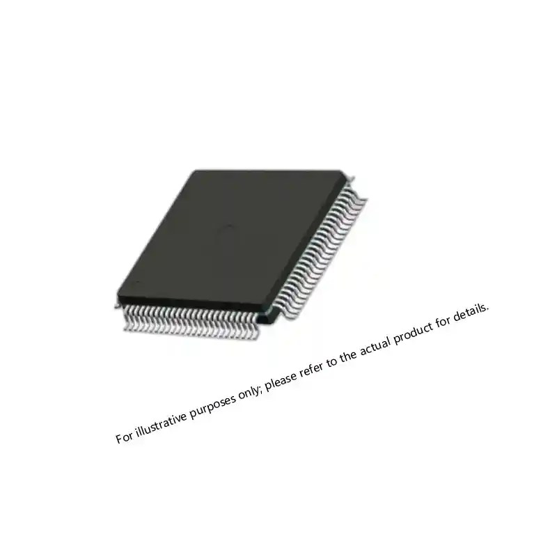
The acquisition of Microsemi by Microchip has not changed the fundamental qualification flows, but it has introduced new document formats. Factory certificates may now carry Microchip letterhead, which sometimes causes confusion during customer audits. We advise including a note in your procurement file explaining the corporate transition to prevent non-conformance reports during quality audits.
Key Considerations for Engineers and Procurement Teams
Do ProASIC3 and SmartFusion2 remain in production after the Microchip acquisition?
Many of the most popular densities remain active, but some older ProASIC variants have moved to mature status. The factory still accepts orders for those parts, but lead times can stretch beyond 20 weeks, and there is no commitment for new wafer starts. For new designs, we generally recommend basing on active parts like the ProASIC3E and SmartFusion2 families, which have clear roadmaps and better allocation.
How do I confirm that a part is QML Class Q rather than just industrial temperature?
The marking and the order code tell the story. QML-qualified parts carry the appropriate slash sheet designation in the documentation, not just on the label. A part number that reads “A3P1000-FGG484I” might be industrial-tested only, while the military version will have a different ordering suffix or be explicitly listed as QML on the certificate. Always match the full order code and the manufacturer’s qualification record, and do not accept that a part is military grade without documentation.
What is the maximum I/O count I can get in a single SmartFusion2 device?
The largest SmartFusion2 packages, such as the FCG1152, can support over 500 user I/O pins, with multiple voltage banks to interface with both legacy 5 V and modern low-voltage peripherals. The I/O flexibility allows you to integrate many board-level functions, but you should verify that the specific pin-out can be sustained in production because factory standard pin-outs sometimes change between die revisions.
Is die banking available for long-term programs that use ProASIC3E devices?
Die banking is available for program volumes that justify a wafer reservation. We have coordinated die banking agreements where a defense prime contractor reserved a specific wafer lot for the duration of a 15-year program, drawing packaged parts as needed. The arrangement requires negotiation with the factory and a commitment to minimum draws, but it is the only guaranteed method for very long sustainment programs.
How quickly can I get a response on an RFQ for a mixed BOM that includes both ProASIC and SmartFusion parts?
Sparkle Electronics processes military FPGA RFQs on a priority basis, typically providing availability, pricing, and lead time within 24 hours for standard part numbers. If your BOM includes a mixture of active and mature devices, we can advise on which items may need LTB action and offer alternatives where applicable. Send your part number list and target quantity to xuansc2144@gmail.com for a consolidated quote, and we will confirm stock and documentation status before you commit.
If you’re interested, check out these related articles:
XCKU115 UltraScale FPGA: Powering Critical Defense Systems
XC7VX485T FPGA: Virtex-7 Performance for Defense
Virtex-7 XC7VX690T: Performance, Reliability, and Integration
A1020B-PG84B ACT2 FPGA: Specs, Sourcing, and Availability