
FPGA Pin-Out Compatibility: Military Second-Source Guide
Table of Contents
- What Pin-Out Compatibility Means for Military FPGA Programs
- Reading Between the Datasheet Lines: Pin-Out Variations Across Second Sources
- How to Verify Pin-Out Compatibility Before Committing to a Second Source
- Qualifying Second‑Source FPGAs for MIL‑SPEC and QML Compliance
- Managing Supply Chain Risk During the Second‑Source Transition
- Common Questions About Military FPGA Second‑Sourcing
FPGA pin-out compatibility is a critical factor when defense programs evaluate second-source alternatives. A pin-out mismatch can delay a production run by months, force a board respin, or compromise the qualified configuration of a fielded system. Drawing on over a decade of sourcing military-grade FPGAs for defense contractors, I have seen how a disciplined verification process—grounded in datasheet analysis, qualification status, and traceability—prevents these pitfalls. This article provides a step-by-step approach to managing second-source FPGA transitions with confidence, focusing on pin-out validation, compliance requirements, and supply chain risk reduction.
What Pin-Out Compatibility Means for Military FPGA Programs
In commercial design, a pin-out change might trigger a quick schematic update and a revised bill of materials. For a fielded defense system, the consequences are far heavier. Every pin position on a military FPGA has been validated through qualification testing, thermal analysis, and signal integrity simulations. Changing even one I/O assignment can require re-qualification of the entire board assembly.
The MIL-PRF-38535 and MIL-STD-883 environments that govern these devices demand that any substitution—even between parts that share a generic part number—preserves mechanical, electrical, and thermal behavior exactly. I have seen programs lose months re‑verifying an assembly because a second-sourced FPGA turned out to have a slightly different ground pad pattern that shifted thermal impedance just enough to push junction temperatures beyond the derated limit. That kind of discovery erodes schedule margin fast.
Three factors make pin-out compatibility particularly challenging in the military segment: package variants across temperature ranges, differences in lead finish plating, and subtle pin-out re‑arrangements between speed grades within the same family. Each one can break drop‑in interchangeability unless checked explicitly.
Reading Between the Datasheet Lines: Pin-Out Variations Across Second Sources
When procurement teams tell me a second‑source FPGA is “form, fit, and function identical,” I ask them to walk through the datasheet comparison at the pin level. A part number like A3P1000‑FGG484 might appear identical across two authorized sources, but the mechanical drawing often reveals differences in the stand‑off height or solder ball composition that affect board‑level reliability.
Even within a single manufacturer’s product line, pin‑out compatibility is not guaranteed across all ordering options. The table below highlights the parameters that most frequently diverge between first‑source and second‑source FPGAs.
| Parameter to Check | Potential Variation | Impact on Compatibility |
|---|---|---|
| Package type (FG, FG G, CSG, CQ) | Ball grid pitch, substrate material | Mechanical fit, thermal path |
| Speed grade | I/O timing, power‑on surge sequencing | Signal integrity, power supply design |
| Temperature range (‑I vs. ‑M) | Pin‑out may shift for extended‑range parts | Board layout, passive component values |
| Lead finish (SnPb vs. RoHS) | Solder process, whisker mitigation | Long‑term reliability, conformal coating adhesion |
| Qualification level (QML Q vs. QML V) | Burn‑in coverage, screening level | Compliance documentation, lot traceability |
A common trap is assuming that a commercial‑grade FPGA with the same base part number will be pin‑compatible with the military version. The die may be the same, but the package substrate, bond‑out, and pin assignment list are often modified for the extended temperature and reliability requirements. If your program uses a die‑banked Part Number Control Specification, the second‑source candidate must match the exact drawing revision, not just the generic device type.
How to Verify Pin-Out Compatibility Before Committing to a Second Source
The verification sequence I use with defense programs starts with the mechanical package drawing. I overlay the first‑source and second‑source drawings and confirm that every ball or lead position, including the body size, stand‑off height, and coplanarity tolerance, is within the board assembly’s allowed window. If the second source uses a different package suffix—for example, FG484 vs. FGG484—I flag it immediately and request a sample for physical fit check.
Next, I compare the pin assignment tables column by column, not just the pin count. A surprising number of discrepancies hide in the power and ground pins. A second‑source FPGA might relocate a quiet digital ground to a different ball position, creating a noisy return path that was not anticipated in the original layout. Signal pins also change: an LVDS pair that was bank‑adjacent in the original may move to a different I/O bank with different VCCIO support, breaking the I/O standard compatibility.
If your program already has an approved vendor list and a qualified assembly, the safest path is to request a formal Conformance Inspection Report from the second‑source supplier that maps every pin to your existing netlist. Distributors with experience in military FPGA sourcing can coordinate this cross‑reference with both the end customer and the factory, saving the program weeks of engineering effort. At Sparkle Electronics, we routinely assist defense contractors in building these pin‑level compliance packages for Actel, Xilinx, and Altera military devices.
Qualifying Second‑Source FPGAs for MIL‑SPEC and QML Compliance
Pin‑out compatibility alone is not enough. The second‑source device must carry the same qualification pedigree as the original. If the original FPGA was procured to MIL‑PRF‑38535 Class Q or Class V, the replacement must hold a valid QML certificate for that exact ordering part number. A 5962‑series part number embeds the qualification status in its coding, so comparing the full SMD number is a quick first filter.
Traceability documentation is what separates a qualified second source from a risky substitution. I always require a Certificate of Conformance that tracks the lot date code, assembly site, and test facility, plus a certified test report showing the same screening flow as the original. For die‑banked programs, the second source must demonstrate that the stored wafers came from the same qualified fabrication process, and that the assembly and test flow is re‑qualified to match the original approved baseline.
One reality that catches buyers off guard: even when a second‑source FPGA is pin‑compatible and qualification‑matched, the lead time may not be. Second‑source production runs are often scheduled infrequently, and allocations can swing based on fab loading. Factoring in a buffer for these scheduling gaps is part of the overall risk assessment.
If the evaluation of compliance documentation feels outside your team’s bandwidth, it is worth bringing in a distributor who handles these documentation packages regularly. We have pulled together detail‑by‑detail qualification packages for Actel A54SX‑A, AX, and ProASIC families, as well as Altera Cyclone and Stratix military variants, so engineering teams can validate the paper trail without starting from scratch.
Managing Supply Chain Risk During the Second‑Source Transition
A successful second‑source transition is not a one‑time part qualification. It is a supply chain posture shift. I have watched programs treat the second source as a passive backup and then find that the source has gone obsolete or that the remaining inventory is tied up in a long‑running allocation. The more robust approach is to establish a dual‑sourcing plan that includes minimum order quantities at the second source, shared forecast data, and pre‑negotiated priority for future wafer starts.
Die banking remains the strongest long‑term hedge. By purchasing and storing tested wafers or finished die, a program can decouple the manufacturing schedule from the immediate demand. The second‑source relationship then becomes about who controls the wafer inventory and can guarantee assembly capacity when the program calls up parts. For high‑density FPGAs like the Axcelerator AX1000‑CQ352M or the APA300‑CQ208B, having a die bank in place removes the single biggest program risk: a discontinued manufacturing line with no drop‑in replacement.
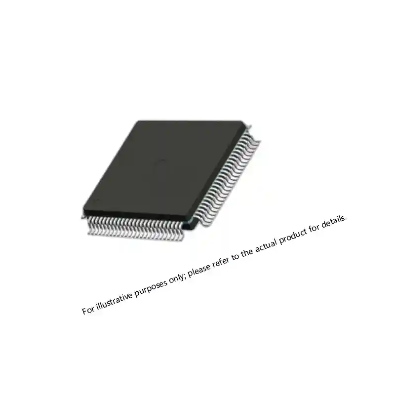
I also recommend keeping a small batch of the second‑source FPGAs in stock for immediate testing. When a field failure or an urgent production lot demands a fast substitution, having pre‑qualified parts on the shelf cuts the response time from months to days. The inventory carrying cost is trivial compared to the cost of a halted production line.
Distributors with deep military FPGA stock can serve as that buffer. At Sparkle Electronics, we carry a wide range of Actel, Altera, and Xilinx military FPGAs that are already traceable and documented, so programs can pull parts immediately while the formal dual‑source qualification is underway.
Common Questions About Military FPGA Second‑Sourcing
Can a commercial‑grade FPGA with the same base part number be used as a drop‑in replacement for a military‑grade device?
In almost every case, no. The die might be the same, but the package, pin‑out, screening, and qualification trace are different. A commercial FPGA will not have the QML certificate, the extended temperature characterization, or the burn‑in data that the military version carries. Even if it powers up correctly on a bench, it cannot satisfy the compliance and reliability requirements of a defense program. If a program is forced to consider a commercial part due to obsolescence, the path forward is an upscreening program with full documentation, not a drop‑in substitution.
What is the single most overlooked pin‑out difference when switching to a second‑source FPGA?
The power and ground ball assignments. Because these nets are often treated as a common plane, many design teams do not check individual ball positions. A second‑source FPGA might distribute power and ground pins differently, even if the total count matches. That can create unexpected current density hotspots or shift the return path for high‑speed signals, degrading signal integrity in ways that pass‑by functional tests do not catch immediately. I always compare the power‑ground pin map one ball at a time.
How does the temperature range affect pin‑out compatibility?
Extended temperature range FPGAs (‑M or ‑I suffix) sometimes use a different package substrate or bond‑out to handle the wider thermal cycling. This can change the pin‑out list even within the same generic part number. The mechanical drawing and the ordering information table will indicate whether the package suffix changes with temperature grade. If the suffix is different, assume the pin‑out requires re‑verification.
What documentation should I expect from a second‑source supplier before qualifying an FPGA?
You should receive at minimum: a Certificate of Conformance with lot date code and assembly site, a certified test report covering the same screening flow as the original device, a QML certificate for that exact part number, and a complete datasheet package that includes the mechanical drawing and pin assignment table. For die‑banked parts, also request the wafer lot traceability and assembly qualification report. If any of these documents is missing or seems generic, the part should not be considered qualified.
Is it better to work with a distributor or go directly to the FPGA manufacturer for a second source?
Both paths can work, but a specialized military component distributor often brings faster cross‑referencing, smaller minimum order quantities, and access to inventory from multiple approved sources. Manufacturers may prioritize large OEM contracts, leaving smaller programs with long lead times. A distributor that carries multiple military FPGA lines can also provide unbiased pin‑out comparisons across brands, which a single manufacturer cannot always do. If you are managing a critical second‑source transition, share your part number and current compliance requirements with our team—we will confirm traceability and provide a pin‑out comparison to accelerate your qualification cycle.
If your program is navigating a second‑source FPGA transition and you need pin‑out verification backed by full traceability, send your target part numbers and quantity requirements to xuansc2144@gmail.com. We will provide a detailed datasheet comparison, qualification status, and immediate availability for the military FPGAs you depend on.
If you’re interested, check out these related articles:
Virtex-7 690T FPGA: Performance, Packaging, and Reliability Insights
XCKU115 UltraScale FPGA: Powering Critical Defense Systems
XC7VX485T Virtex-7 FPGA: Performance and Sourcing for Defense