
TPS73633MDBVREP 400mA 3.3V LDO: EP-Grade SOT-23-5 Guide
Table of Contents
- TPS73633MDBVREP: Electrical, Thermal, and Package Profile
- What the EP Grade and V62 Baseline Actually Mean
- Need the V62 Drawing and Lot-Specific Documentation?
- ESD, Moisture Sensitivity, and Thermal Verification
- Application and Layout Considerations for 3.3 V Rails
- Sourcing, Traceability, and Incoming Inspection
- Request a BOM-Level Quote with Documentation Requirements
- Get a Verified Quote for TPS73633MDBVREP
- Frequently Asked Questions
- What is TPS73633MDBVREP?
- What does the EP suffix mean for military projects?
- What input voltage should I provide for a clean 3.3 V output?
- Is TPS73633MDBVREP a QML or radiation-hardened device?
- Does the EP part include reverse-current protection?
- References
Designers selecting a compact, low-noise rail for defense-grade analog and digital circuitry keep returning to TPS73633MDBVREP. It is a fixed 3.3 V, 400 mA low-dropout linear regulator in a 5-pin SOT-23 (DBV) package, supplied under an Enhanced Product baseline with extended verification and documentation controls [1]. The part is used where stable output voltage, reverse-current isolation, small footprint, and predictable temperature behavior matter more than lowest unit cost.
For a 3.3 V rail, the device fits naturally between a 5 V or intermediate front-end rail and the load. Its SOT-23-5 footprint simplifies layout in sensor channels, FPGA support rails, analog front ends, and single-board computers. But the reason hi-rel programs treat it as more than a commercial LDO is the EP suffix: the controlled baseline changes what purchasers receive in terms of documented reliability, source control, and change notification [1].
TPS73633MDBVREP: Electrical, Thermal, and Package Profile
| Parameter | Published characteristic | Design impact |
|---|---|---|
| Output voltage | 3.3 V fixed | Total output tolerance is controlled across line, load, and temperature; verify the exact band against the current lot documentation. |
| Continuous output current | 400 mA | Sized for point-of-load analog and digital rails, not board-level bulk power. |
| Dropout voltage | Approximately 75 mV typical; maximum limit specified at 400 mA | The input must remain above VOUT plus dropout. For 3.3 V output at full load, practical minimum input is about 3.5 V. |
| Input voltage range | 1.7 V–5.5 V for the family | The fixed 3.3 V version operates with input voltage above the output plus dropout. |
| Shutdown current | Less than 1 µA typical with EN low | Supports sequenced power-down and low quiescent standby modes. |
| Reverse-current protection | Internal PMOS isolation | Helps prevent current from the output capacitor flowing back into a collapsed input rail. |
| Package | SOT-23-5 (DBV) | Compact nonhermetic package; use an IPC-compliant land pattern [7]. |
| Operating junction temperature | -55°C to +125°C | Enhanced Product baseline covers the extended temperature range. |
The published electrical limits should be checked against the controlled drawing for the specific date and lot code. Do not mix limits from the commercial TPS736 device with the Enhanced Product unless the program has formally accepted that substitution.
What the EP Grade and V62 Baseline Actually Mean
Enhanced Product, or EP, is not simply a temperature-bin decision. It is a controlled baseline approach: reduced variation in assembly and test, extended temperature characterization, qualification documentation, and change notification when material or process changes occur [1]. For defense purchasing teams, that converts into evidence that can be placed into an incoming inspection file.
The Defense Logistics Agency maintains a Vendor Item Drawing for this device under V62/12608-01XE [1]. The drawing gives designers a referenceable procurement baseline when a full QML-level SMD is not required. This is different from a device certified to MIL-PRF-38535. A QML part carries qualification under the military performance specification for monolithic microcircuits [2]; an EP part uses a vendor-controlled baseline with documented electrical and environmental testing suitable for many defense and industrial applications. Program flow-down determines which level is required.
Need the V62 Drawing and Lot-Specific Documentation?
Before committing a design, request the full drawing, qualification summary, and current revision status. Email the part number and your program’s required temperature grade to xuansc2144@gmail.com, and Sparkle will return the applicable documentation options.
ESD, Moisture Sensitivity, and Thermal Verification
Because the package is nonhermetic plastic, three verification areas require attention before production release: electrostatic discharge, moisture sensitivity, and thermal resistance.
The device’s ESD classification is characterized using JEDEC test methods for human body model and charged device model event levels [3][4]. The exact classification for the current production lot should be confirmed from the qualification report rather than assumed from a commercial datasheet. For most analog LDOs in this package class, HBM and CDM levels are sufficient for standard ESD-protected handling, but the program’s ESD control plan should still be applied.
Moisture sensitivity is classified under IPC/JEDEC J-STD-020 for nonhermetic surface-mount devices [5]. The relevant MSL level must be verified before reflow. If the part absorbs moisture beyond the floor-life limit, baking may be required before placement. Sparkle’s incoming documentation should include the MSL rating and any handling instructions for the reel or tray.
Thermal performance is measured using the electrical test method described in JEDEC JESD51-1 [6]. Junction temperature rise depends on power dissipation, which is approximately (VIN – VOUT) × IOUT. At 400 mA with a 1.7 V differential, dissipation is about 0.68 W. The designer must evaluate copper area, adjacent components, and board stack-up to keep the junction within the -55°C to +125°C range.
Application and Layout Considerations for 3.3 V Rails
Stable LDO performance starts at the board level. Keep the input and output capacitors close to the package, with the ground return routed directly to the GND pin. The noise-reduction pin should be populated with the manufacturer-recommended capacitor value if lower output noise is required. Do not leave the enable pin floating; tie it to a logic-level source or pull it high through the recommended resistance when the rail is always on.
The TPS73633MDBVREP is a useful clean-rail isolator for mixed-signal loads that cannot tolerate switching noise from an upstream DC-DC converter. It works best as a local regulator for ADC references, PLL supplies, sensor bias, and low-current FPGA auxiliary rails. The low dropout keeps heat low in tightly packed enclosures.
When the design expands from analog power to dense digital processing, the same supply-chain discipline applies at the board level. Power integrity, packaging constraints, and sequencing become visible only when the full BOM is reviewed.
For high-density defense FPGA platforms, supply rail planning becomes more complex across multiple core and auxiliary voltages. <XCKU115 UltraScale FPGA: Powering Critical Defense Systems> covers how mission-critical processing cards handle performance, packaging, and integration.
When the program moves beyond analog power to specification-level digital processing, <UltraScale KU085 FPGA Specifications for Defense Systems> covers how to evaluate device specifications for defense systems.
Sourcing, Traceability, and Incoming Inspection
For a high-reliability LDO, sourcing is documentation work as much as inventory work. At minimum, request a Certificate of Conformance, the V62/12608-01XE alignment evidence, date and lot code, and the current revision of the qualification summary [1]. If the program requires AS9120 flow-down, confirm that the supplier’s incoming inspection record includes visual inspection, package marking verification, and reel/tray condition checks.
Representative high-reliability product images used for incoming-inspection records across the Sparkle catalog include 
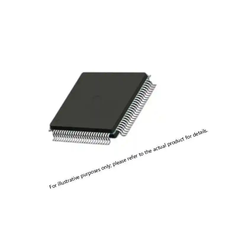
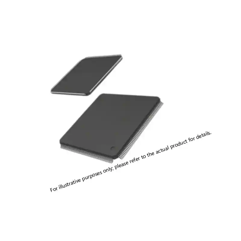
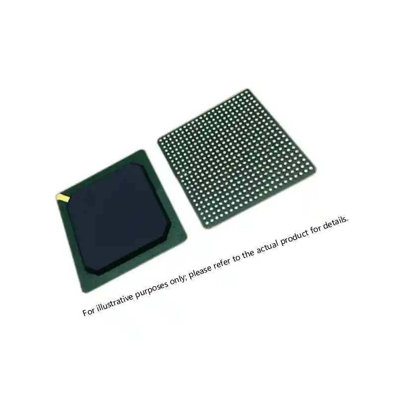
Sparkle stocks this part within its Analog & Signal Chain category, alongside power modules, precision amplifiers, and voltage references. Incoming verification focuses on pin-one orientation, body marking, and reel integrity before the lot is released.
For a comparable spec-guide treatment of a high-reliability programmable device, <A1020B-PG84B ACT2 FPGA: Specs, Sourcing, and Availability> covers how part-number decoding, package verification, and sourcing choices affect program risk.
Request a BOM-Level Quote with Documentation Requirements
Send the quantity, target date, and documentation list to xuansc2144@gmail.com. Sparkle checks current stock, V62 revision alignment, and inspection data before quoting, so there are no surprises at incoming inspection.
Get a Verified Quote for TPS73633MDBVREP
Sparkle Electronics supports BOM-level sourcing for hi-rel LDOs, power modules, and related analog signal chain components. Submit the part number, required date, quantity, and documentation requirements to xuansc2144@gmail.com. A specialist will reply with availability, pricing, and a documentation path that matches your incoming inspection procedure.
Frequently Asked Questions
What is TPS73633MDBVREP?
TPS73633MDBVREP is a fixed 3.3 V, 400 mA low-dropout linear regulator in a 5-pin SOT-23 package, supplied under an Enhanced Product baseline with extended temperature documentation and a controlled change flow [1].
What does the EP suffix mean for military projects?
EP indicates a controlled baseline with extended temperature range, qualification documentation, and change notification. It is not automatically the same as full QML certification under MIL-PRF-38535 [2]. The program’s flow-down determines whether EP is acceptable.
What input voltage should I provide for a clean 3.3 V output?
The input must remain above the output voltage plus dropout. At 400 mA, the practical minimum input is approximately 3.5 V. A 3.7 V or 5 V rail is typically used depending on the upstream supply.
Is TPS73633MDBVREP a QML or radiation-hardened device?
No. It is an Enhanced Product with a DLA Vendor Item Drawing. It is not a QML-certified part and it is not radiation-hardened. For space or radiation-sensitive programs, the component should be evaluated against the applicable QML, rad-hard, or radiation-tolerant requirements.
Does the EP part include reverse-current protection?
Yes. The device includes reverse-current protection to help prevent current from the output capacitor flowing back toward the input, which is useful when the input rail may be switched off or collapse during power sequencing.
References
[1] DLA Land and Maritime, Vendor Item Drawing V62/12608-01XE, TPS73633MDBVREP Enhanced Product, current revision.
[2] U.S. Department of Defense, MIL-PRF-38535, General Specification for Integrated Circuits (Microcircuits) Manufacturing.
[3] JEDEC, JESD22-A114, Electrostatic Discharge (ESD) Sensitivity Testing Human Body Model (HBM).
[4] JEDEC, JESD22-A115, Electrostatic Discharge (ESD) Sensitivity Testing Charged Device Model (CDM).
[5] IPC/JEDEC, J-STD-020, Moisture/Reflow Sensitivity Classification for Nonhermetic Surface-Mount Devices.
[6] JEDEC, JESD51-1, Integrated Circuit Thermal Measurement Method—Electrical Test Method.
[7] IPC, IPC-7351, Generic Requirements for Surface Mount Design and Land Pattern Standard.
If you’re interested, check out these related articles:
XC7VX485T FPGA: Virtex-7 Performance for Defense
Virtex-7 690T FPGA: Performance, Packaging, and Reliability Insights
XCKU085 UltraScale FPGA: Performance for Critical Systems
XC7VX485T Virtex-7 FPGA: Performance and Sourcing for Defense