XCZU47DR: Zynq RFSoC for High-Performance RF Systems
Table of Contents
- What the XCZU47DR-2FFVG1517I Actually Contains
- Why the -2 Speed Grade Matters for Wideband RF Applications
- How RFSoC Integration Changes Board-Level Design
- Where the XCZU47DR-2FFVG1517I Fits in Mission-Critical Systems
- Procurement Considerations for High-Reliability RFSoC Applications
- Frequently Asked Questions
- What does the -2 speed grade indicate for the XCZU47DR-2FFVG1517I?
- How does the Zynq UltraScale+ RFSoC architecture reduce system complexity?
- Can the XCZU47DR-2FFVG1517I operate in harsh environmental conditions?
- What development tools support the XCZU47DR-2FFVG1517I?
The XCZU47DR-2FFVG1517I sits at the intersection of direct RF conversion and programmable logic, a combination that has reshaped what fits inside a single enclosure for radar, 5G infrastructure, and electronic warfare platforms. This Zynq UltraScale+ RFSoC variant packs RF-ADCs, RF-DACs, an ARM Cortex-A53 quad-core processor, and a substantial FPGA fabric onto one die. For engineers working on systems where board space, power budget, and latency all compete for priority, the integration density here changes the design calculus in ways that discrete component approaches simply cannot match.
What the XCZU47DR-2FFVG1517I Actually Contains
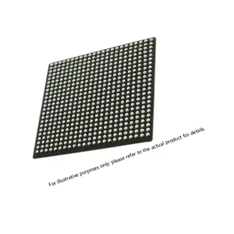
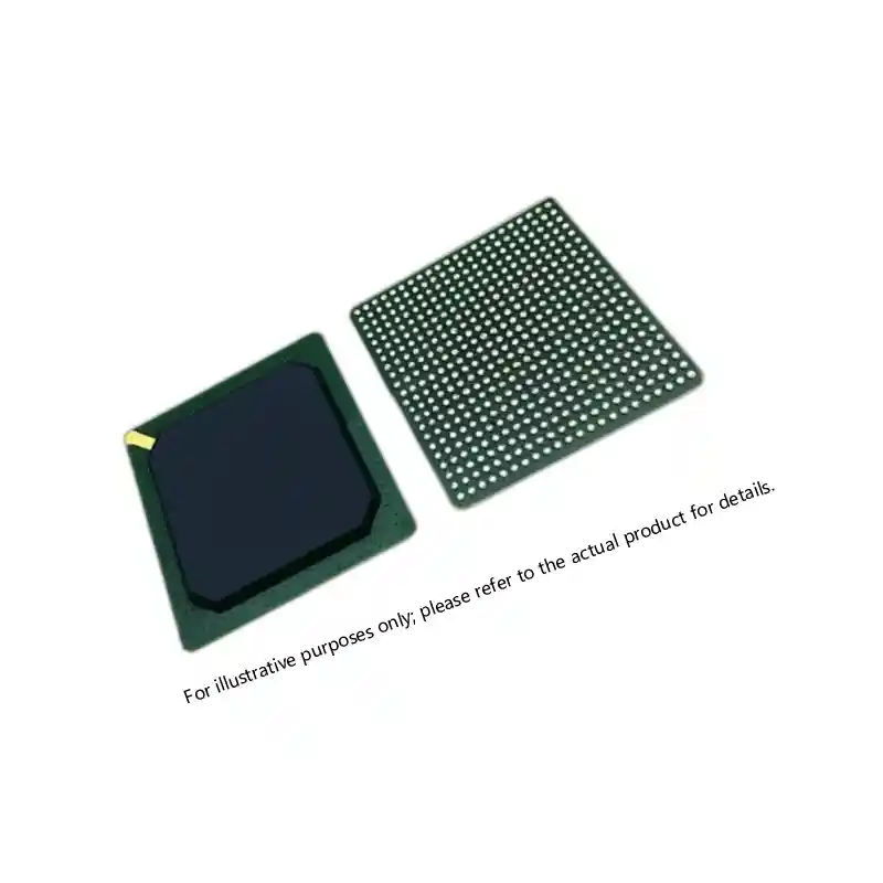
The XCZU47DR-2FFVG1517I is a Zynq UltraScale+ RFSoC, meaning it combines three distinct processing domains on a single substrate. The processing system (PS) provides general-purpose computing through an ARM Cortex-A53 quad-core cluster, handling control logic, protocol stacks, and embedded Linux operations. The programmable logic (PL) section functions as an FPGA fabric where custom digital signal processing chains, beamforming algorithms, and digital pre-distortion (DPD) blocks can be implemented in parallel. The third domain, and the one that defines the RFSoC category, consists of integrated RF data converters. These RF-ADCs and RF-DACs sample and synthesize signals directly at RF frequencies, bypassing the intermediate frequency stages that traditional architectures require.
| Feature | Specification |
|---|---|
| Device Family | Zynq UltraScale+ RFSoC |
| Part Number | XCZU47DR-2FFVG1517I |
| Processing System | ARM Cortex-A53 quad-core |
| Programmable Logic | UltraScale+ FPGA architecture |
| RF Converters | Integrated RF-ADC and RF-DAC |
| Speed Grade | -2 (high performance) |
| Temperature Grade | Industrial (-40°C to +100°C) |
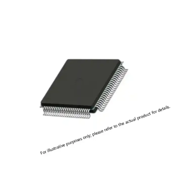
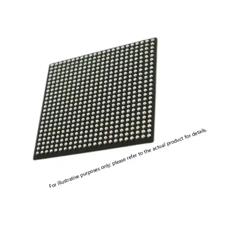
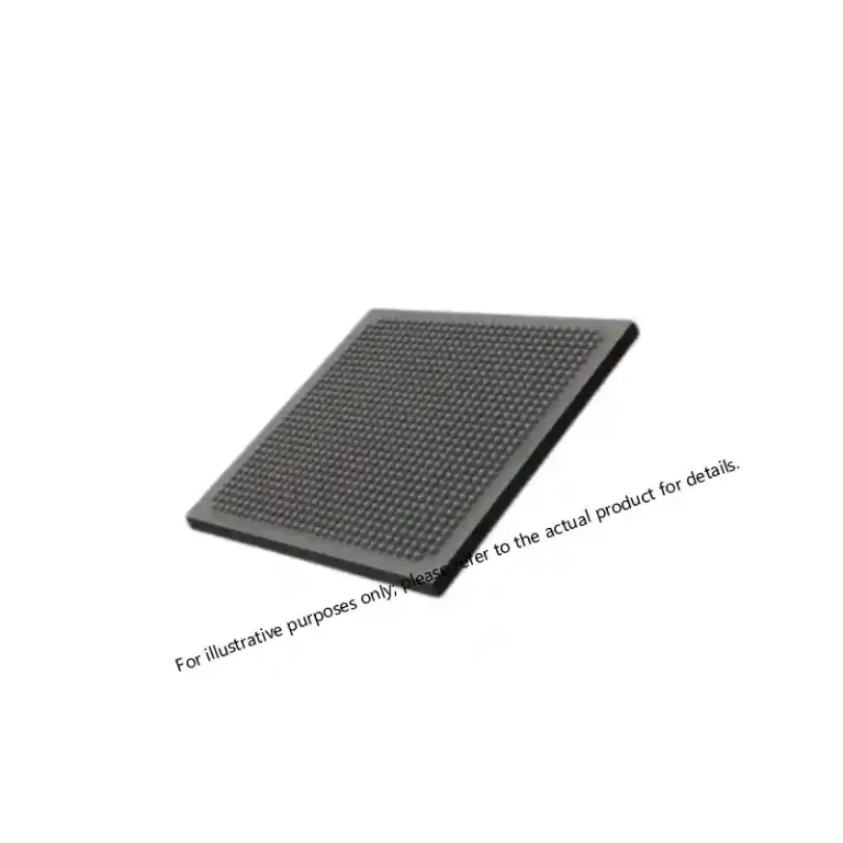
| Package | FFVG1517 |
The heterogeneous computing model here is not marketing language. It reflects a genuine architectural split where latency-critical operations run in hardware while supervisory functions execute on the ARM cores. This division matters when processing wideband RF signals where microseconds of additional delay can degrade system performance.
Why the -2 Speed Grade Matters for Wideband RF Applications
Speed grade designations on Xilinx devices indicate tested and guaranteed performance limits for internal logic timing. The -2 designation on the XCZU47DR-2FFVG1517I means the device has been characterized for higher clock frequencies than -1 grade parts, with correspondingly tighter timing margins on critical paths.
For signal processing applications, this translates directly into achievable sample rates and algorithm complexity. A beamforming implementation that requires 400 MHz internal clocks will not meet timing on a slower speed grade, regardless of how carefully the RTL is written. The -2 grade provides headroom for demanding designs where the processing chain must keep pace with high-bandwidth RF data converters operating at multi-gigasample rates.
The practical impact shows up in several ways. Wider instantaneous bandwidth becomes feasible because the digital backend can process more samples per second. More sophisticated algorithms fit within the latency budget because each processing stage completes faster. Power consumption per operation can actually decrease because the logic runs at higher efficiency points rather than being stretched across multiple clock cycles.
In radar applications, where range resolution depends on signal bandwidth and target detection depends on processing latency, the -2 speed grade is often a hard requirement rather than a preference. Similar constraints apply in electronic warfare systems where threat identification must happen within strict time windows.
How RFSoC Integration Changes Board-Level Design
Traditional RF systems separate the analog front end, data conversion, and digital processing across multiple devices and often multiple boards. Each interface between components introduces latency, consumes power, and requires careful impedance matching. The XCZU47DR-2FFVG1517I collapses this distributed architecture into a single device.
The system integration benefits are measurable. Board area decreases because the discrete ADCs, DACs, and their supporting circuitry disappear. Power consumption drops because the on-chip data paths between converters and processing logic consume far less energy than board-level traces and external interfaces. Design complexity reduces because the number of high-speed interfaces requiring careful layout shrinks dramatically.
Hardware-software co-design becomes more tractable when the processing system and programmable logic share the same silicon. The ARM cores can configure and monitor the FPGA fabric through internal interfaces rather than external buses. Data can move between the PS and PL domains with minimal latency, enabling software control of hardware accelerators without the overhead of traditional processor-FPGA communication.
Development workflows benefit from this integration as well. The Vivado Design Suite handles the hardware implementation while the Vitis unified software platform manages embedded software development. Both tools understand the RFSoC architecture natively, providing simulation models and debugging capabilities that span the hardware-software boundary. An RFSoC development board allows prototyping and validation before committing to a custom board design.
Where the XCZU47DR-2FFVG1517I Fits in Mission-Critical Systems
The combination of RF conversion, programmable logic, and processing power in a single industrial temperature grade device opens applications that previously required rack-mounted equipment.
In 5G wireless infrastructure, the XCZU47DR-2FFVG1517I handles the digital front end for massive MIMO base stations. The RF-DACs generate the transmit waveforms while the RF-ADCs capture the receive signals, and the FPGA fabric implements the beamforming and digital pre-distortion algorithms that make high-order modulation practical. The ARM cores manage the protocol stack and interface with the network controller.
Radar systems benefit from the wideband RF capabilities and low-latency processing. A phased array radar can implement adaptive beamforming in the FPGA fabric while the ARM cores handle target tracking and display functions. The integrated architecture allows the entire signal chain from antenna to processed output to fit in a single module.
Software-defined radio (SDR) platforms use the RFSoC as a universal transceiver. The same hardware can implement different waveforms by changing the FPGA configuration and software, enabling multi-mode radios that adapt to operational requirements. This flexibility is particularly valuable in electronic warfare applications where threat environments evolve faster than hardware development cycles.
In a recent project supporting a defense contractor developing next-generation electronic warfare systems, the RFSoC-based architecture reduced the overall system footprint by 30% compared to the previous discrete implementation while achieving a 2x improvement in signal processing throughput. The smaller form factor allowed installation on platforms where the legacy system would not fit, directly expanding operational capability.
For aerospace and defense applications, the availability of MIL-SPEC components and industrial temperature grade variants addresses environmental requirements that commercial parts cannot meet. The XCZU47DR-2FFVG1517I operates across the -40°C to +100°C industrial temperature range, covering most airborne and ground-based military environments.
Procurement Considerations for High-Reliability RFSoC Applications
Sourcing the XCZU47DR-2FFVG1517I for defense and aerospace programs involves considerations beyond technical specifications. Authenticity verification matters because counterfeit components in mission-critical systems create unacceptable risk. Traceability documentation must support program requirements for component history and handling. Supply chain security increasingly requires visibility into the chain of custody from manufacturer to end user.
Long-lifecycle programs face obsolescence management challenges. A radar system with a 20-year service life will outlast the production run of most semiconductor components. Planning for last-time buys, qualifying alternate sources, and maintaining inventory require coordination between program managers and component suppliers.
SPARKLE ELECTRONICS CO., LIMITED works with defense contractors and systems integrators on these procurement challenges. We provide authenticated components with full traceability documentation and support obsolescence management planning for programs using specialized RFSoCs like the XCZU47DR-2FFVG1517I.
Frequently Asked Questions
What does the -2 speed grade indicate for the XCZU47DR-2FFVG1517I?
The -2 speed grade indicates the device has been tested and qualified for higher clock frequencies and faster internal timing than lower speed grades. This matters for applications requiring maximum processing throughput, such as wideband radar signal processing or high-bandwidth 5G implementations. The faster logic allows more complex algorithms to execute within latency budgets that slower devices cannot meet.
How does the Zynq UltraScale+ RFSoC architecture reduce system complexity?
The architecture integrates RF data converters, programmable logic, and an ARM processing system on a single die. This eliminates the board-level interfaces between discrete ADCs, DACs, FPGAs, and processors that traditional architectures require. Fewer high-speed interfaces mean simpler board layouts, lower power consumption, and reduced design risk. The shared silicon also enables tighter hardware-software integration through internal data paths rather than external buses.
Can the XCZU47DR-2FFVG1517I operate in harsh environmental conditions?
The XCZU47DR-2FFVG1517I is specified for the industrial temperature range of -40°C to +100°C, covering most military ground and airborne environments. The FFVG1517 package provides robust mechanical and thermal characteristics suitable for high-vibration applications. For programs requiring extended temperature ranges or additional screening, consult with your supplier about available options.
What development tools support the XCZU47DR-2FFVG1517I?
Xilinx provides the Vivado Design Suite for hardware design, including synthesis, implementation, and timing analysis for the FPGA fabric. The Vitis unified software platform handles embedded software development for the ARM processing system, including bare-metal and Linux-based applications. Both tools include simulation models and debugging capabilities specific to the RFSoC architecture. If your project involves complex signal processing requirements, discussing the development approach with an experienced applications team can help avoid common integration issues. Contact SPARKLE ELECTRONICS CO., LIMITED at [email protected] for component sourcing and technical coordination support.
If you’re interested, check out these related articles:
Virtex-7 XC7VX690T: Performance and Reliability Insights
XC7VX485T Virtex-7 FPGA: Performance and Sourcing for Defense
Virtex-7 690T FPGA: Performance for Mission-Critical Systems
XC7VX485T FPGA: Virtex-7 Performance for Defense