SWaP-C Optimization for Military Electronics: Selecting Components for Size
Table of Contents
- Why SWaP-C Drives Military Component Selection
- How Package Selection Affects Size and Thermal Performance
- Selecting FPGAs and Processors for Power Efficiency
- Reducing Weight Through Component Integration and Material Selection
- Balancing Cost Against Size, Weight, and Power
- Advanced Packaging Technologies for Extreme SWaP Constraints
- Component Selection Process for SWaP-C Programs
- Sourcing SWaP-C Optimized Components
- Common Questions About SWaP-C Component Selection
- What is the difference between SWaP and SWaP-C?
- Can commercial components be used in SWaP-C optimized military systems?
- How do I verify that a component meets SWaP-C requirements?
- What qualification levels are available for advanced-package military components?
- How do lead times affect SWaP-C component selection?
- Sources and Further Reading
Every gram and cubic centimeter matters when a defense system must fit inside a missile seeker, a soldier’s wearable radio, or a UAV payload bay. SWaP-C optimization, the discipline of balancing Size, Weight, Power, and Cost in military electronics, determines whether a system meets its operational envelope or fails qualification. The challenge is not simply choosing smaller parts. It is selecting components that maintain full MIL-SPEC performance while reducing physical footprint, thermal load, and program cost simultaneously. From my experience supporting defense programs across radar, avionics, and man-portable systems, the procurement decisions made during component selection define whether SWaP-C targets are achievable or whether redesign becomes inevitable.
Why SWaP-C Drives Military Component Selection
SWaP-C emerged as a formal framework because modern defense platforms face constraints that commercial electronics never encounter. A fighter jet’s avionics bay has fixed volume allocations. A dismounted soldier cannot carry unlimited battery weight. A satellite’s power budget is dictated by solar panel area and orbital geometry. These physical realities mean that component selection is not a downstream procurement task but an upstream system engineering decision.
The four parameters interact in ways that create tradeoffs. Selecting a smaller package often increases thermal density, which demands more power for cooling or forces derating. Choosing a lower-power device may sacrifice processing speed, requiring additional components to meet throughput requirements. Cost enters the equation because MIL-SPEC qualified parts in advanced packages command significant premiums over commercial equivalents.
Defense programs increasingly specify SWaP-C requirements at the subsystem level, flowing down to component specifications. A radar signal processing board might have a 200-gram weight allocation, a 15-watt power ceiling, and a 50-cubic-centimeter volume limit. Meeting all three while maintaining MTBF targets requires component selection that considers package type, power efficiency, thermal characteristics, and qualification level together.
How Package Selection Affects Size and Thermal Performance
Package technology is the most direct lever for size reduction. The same silicon die can be housed in a ceramic dual-inline package consuming 2.5 cubic centimeters or a chip-scale BGA occupying 0.3 cubic centimeters. The difference matters when a design must fit within a 10-centimeter-square board area.
| Package Type | Typical Volume | Thermal Resistance | MIL-SPEC Availability |
|---|---|---|---|
| Ceramic DIP | High | Low (good) | Excellent |
| Ceramic LCC | Medium | Low | Good |
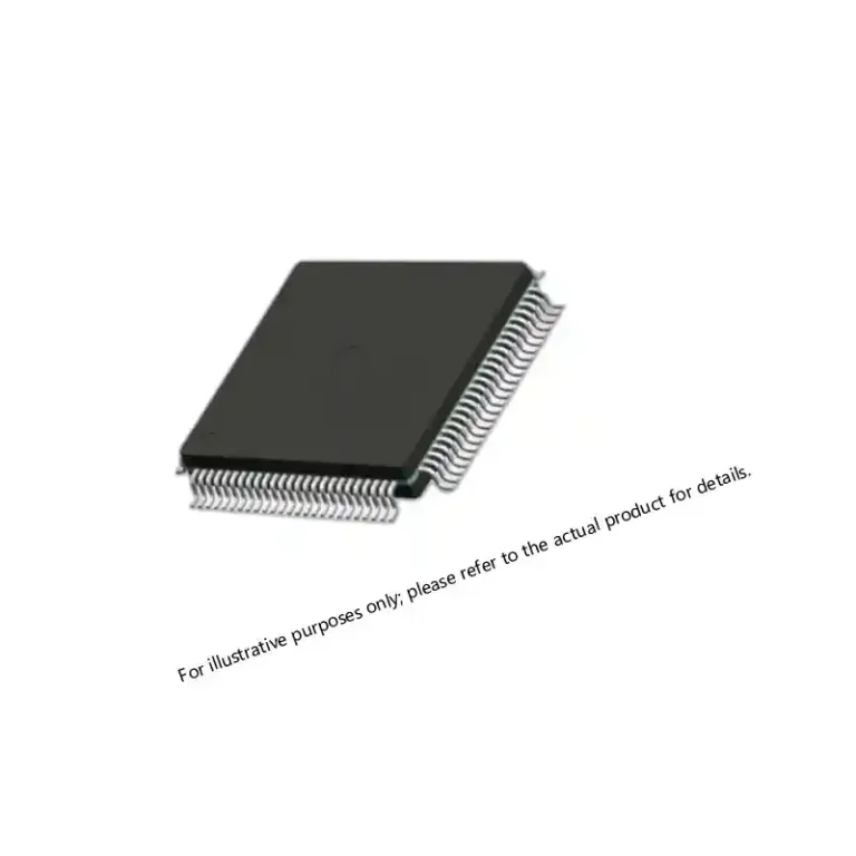
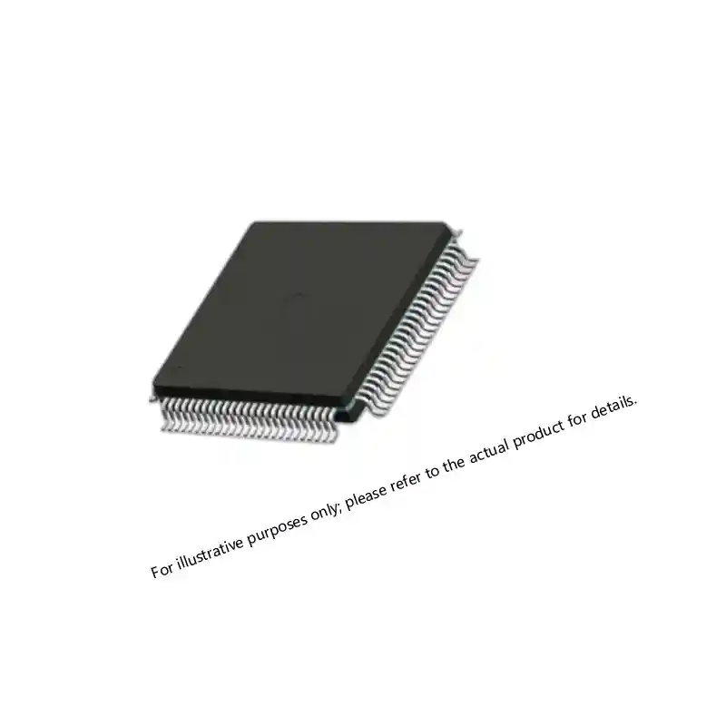
| Plastic QFP | Medium | Medium | Limited |
| Ceramic BGA | Low | Medium | Growing |
| Chip-Scale BGA | Very Low | High (challenging) | Limited |
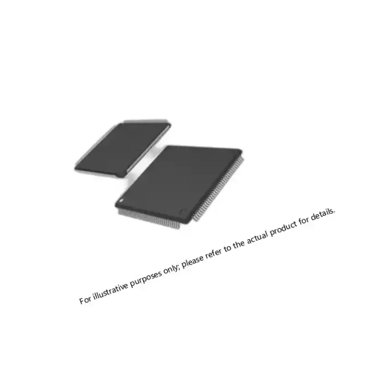
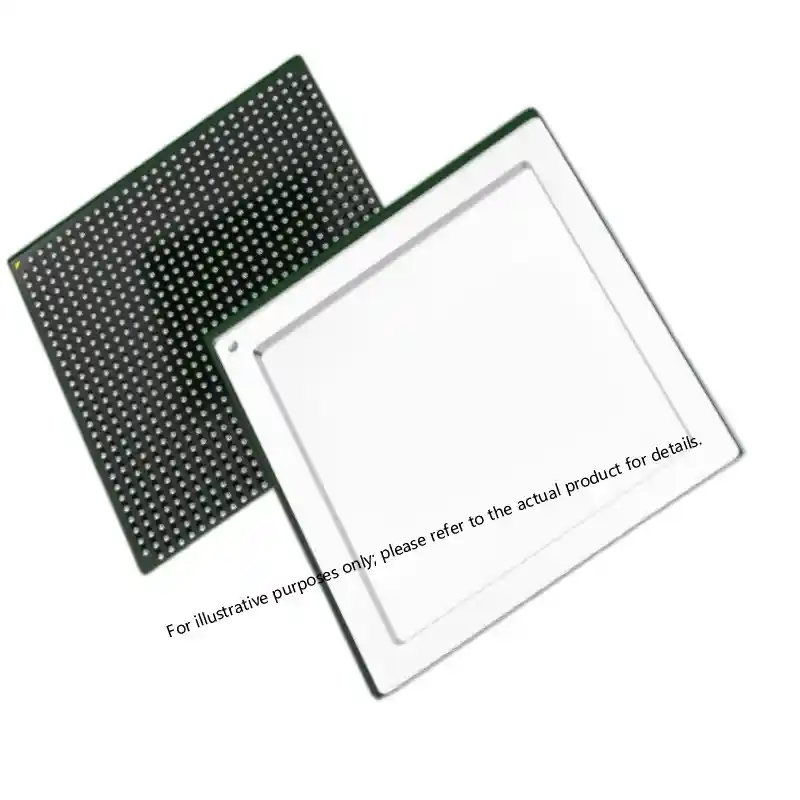
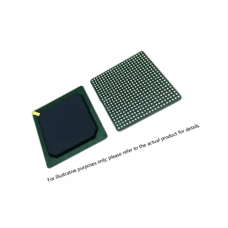
Ceramic packages remain dominant in MIL-PRF-38535 qualified devices because they provide hermetic sealing and superior thermal dissipation. However, ceramic BGAs and land grid arrays now offer significant size reductions while maintaining qualification pathways. The Microsemi PolarFire series, for example, is available in FCSG and FCG packages that reduce board area by 40% compared to earlier generation FPGAs at equivalent gate counts.
Thermal resistance increases as packages shrink because there is less surface area for heat dissipation. A chip-scale package with 0.5mm ball pitch may have junction-to-ambient thermal resistance of 35°C/W compared to 15°C/W for a ceramic flatpack. This means the same power dissipation produces higher junction temperatures, potentially requiring derating or active cooling. When selecting components for SWaP-C optimization, thermal analysis must accompany package selection to verify that smaller packages do not create reliability problems.
Selecting FPGAs and Processors for Power Efficiency
Processing devices typically dominate power budgets in military electronics. An FPGA running complex signal processing algorithms may consume 10 to 50 watts depending on utilization, clock frequency, and process node. Selecting the right device family and configuration is the highest-impact decision for power optimization.
Modern FPGA families offer significant power advantages through advanced process nodes. A Xilinx Kintex UltraScale device at 20nm consumes roughly 50% less dynamic power than a Virtex-5 at 65nm for equivalent logic utilization. The power reduction comes from lower core voltage (0.85V versus 1.0V) and reduced capacitance per logic element.
However, defense programs cannot always adopt the latest process nodes because qualification lags commercial availability. QML-qualified devices typically trail commercial releases by two to four years. A program starting design today may need to select from Virtex-7 or Kintex-7 families rather than UltraScale+ to ensure qualified parts are available when production begins.
Power optimization also depends on design choices beyond device selection. Clock gating, power domains, and algorithm efficiency often contribute more to power reduction than device selection alone. A well-optimized design on a Virtex-7 may consume less power than a poorly optimized design on UltraScale. Component selection should therefore include power analysis at the application level, not just datasheet comparisons.
For programs where power is the primary constraint, devices like the Microsemi SmartFusion2 offer interesting tradeoffs. These parts integrate an ARM Cortex-M3 processor with FPGA fabric and flash memory, eliminating external components while providing low-power modes that can reduce standby consumption to microwatts. The M2S150-FCVG484I, for instance, provides 150K logic elements with total power under 500mW in typical configurations.
Reducing Weight Through Component Integration and Material Selection
Weight reduction in military electronics comes from three sources: component integration, substrate selection, and mechanical design. Component selection directly influences the first two.
Multi-chip modules (MCMs) and system-in-package (SiP) devices integrate multiple die into single packages, eliminating the weight of individual packages, bond wires, and PCB interconnects. A custom MCM containing an FPGA, memory, and power management may weigh 40% less than discrete equivalents while occupying 60% less board area. The tradeoff is higher non-recurring engineering cost and longer lead times, making MCMs appropriate for high-volume programs or extreme SWaP constraints.
Standard integrated devices offer similar benefits without custom development. A processor with integrated memory controller, Ethernet PHY, and power management eliminates multiple discrete components. The NXP QorIQ series, for example, integrates DDR controllers, PCIe interfaces, and Ethernet MACs that would otherwise require separate devices.
Substrate weight becomes significant in large assemblies. Standard FR-4 PCB material weighs approximately 1.85 g/cm³. Polyimide flex circuits weigh 1.42 g/cm³, a 23% reduction. For a 100-square-centimeter board at 1.6mm thickness, the difference is 7 grams. Across a system with 20 boards, substrate selection alone can save 140 grams.
Component selection affects substrate choice because not all devices are compatible with flex circuits or high-temperature laminates. Fine-pitch BGAs require controlled-impedance substrates with tight layer registration. Some MIL-SPEC devices are only qualified on specific substrate materials. Verifying substrate compatibility during component selection prevents redesign later.
Balancing Cost Against Size, Weight, and Power
Cost is the C in SWaP-C, and it often conflicts with the other three parameters. The smallest, lightest, lowest-power solution is rarely the cheapest. Defense programs must determine which parameter takes priority and accept tradeoffs on the others.
MIL-PRF-38535 Class V (space-grade) devices cost 5 to 20 times more than Class B equivalents. QML-qualified parts cost 2 to 10 times more than commercial equivalents. Advanced packages like ceramic column-grid arrays command premiums over standard ceramic flatpacks. A program optimizing purely for size might select a chip-scale BGA that costs three times more than a QFP alternative.
Cost optimization requires understanding total program cost, not just unit component cost. A smaller, more expensive component that eliminates a board or reduces assembly complexity may lower total system cost. A lower-power device that allows a smaller battery or eliminates a cooling fan saves weight and cost elsewhere.
Life-cycle cost also matters for long-duration programs. Selecting a component with a 15-year production commitment avoids obsolescence management costs. Choosing a device with multiple qualified sources reduces supply chain risk premiums. These factors are difficult to quantify during initial selection but significantly affect total program cost.
If your program is balancing SWaP-C priorities across multiple subsystems, it is worth discussing component selection strategies with a distributor who understands both the technical tradeoffs and the supply chain realities. Reach out to xuansc2144@gmail.com with your requirements and constraints.
Advanced Packaging Technologies for Extreme SWaP Constraints
Programs with the most demanding SWaP requirements turn to advanced packaging technologies that go beyond standard surface-mount devices. These technologies offer substantial size and weight reductions but require careful qualification and supply chain planning.
3D packaging stacks multiple die vertically, connected by through-silicon vias (TSVs) or micro-bumps. A 3D-stacked memory device can provide four times the density in the same footprint as a single-die package. High-bandwidth memory (HBM) used in advanced signal processing combines multiple DRAM die with a logic die in a single package, eliminating the board area and power consumption of discrete memory interfaces.
Wafer-level packaging (WLP) eliminates the traditional package entirely, placing solder balls directly on the die. WLP devices can be 90% smaller than equivalent wire-bonded packages. However, WLP creates thermal management challenges because there is no package to spread heat, and the devices are more susceptible to mechanical stress.
Embedded die technology places bare die within PCB substrates, eliminating package height entirely. A processor embedded in the PCB adds zero height to the assembly, compared to 1 to 3mm for a standard BGA. This technology is used in some military applications where height constraints are severe, such as conformal electronics or smart munitions.
These advanced technologies are not yet widely available with MIL-SPEC qualification. Programs considering them must plan for custom qualification testing or accept deviation from standard military specifications. The additional qualification cost and schedule risk must be weighed against the SWaP benefits.
| Technology | Size Reduction | Qualification Status | Typical Applications |
|---|---|---|---|
| 3D Stacking | 50-75% | Limited MIL-SPEC | High-density memory |
| Wafer-Level Package | 80-90% | Emerging | Sensors, RF devices |
| Embedded Die | 70-85% | Custom qualification | Height-critical systems |
| System-in-Package | 40-60% | Growing availability | Integrated subsystems |
Component Selection Process for SWaP-C Programs
Effective SWaP-C optimization requires a structured component selection process that evaluates candidates against all four parameters simultaneously. The process begins with system-level requirements and flows down to component specifications.
First, establish quantitative SWaP-C budgets for each subsystem. A vague requirement to “minimize size” provides no basis for tradeoff decisions. Specific allocations such as “signal processing board shall not exceed 150 grams, 12 watts average power, and 80 cubic centimeters” enable objective evaluation.
Second, identify candidate components that meet functional requirements. For each function, list devices from multiple vendors that provide the required performance. Include both MIL-SPEC qualified parts and commercial parts that might be upscreened.
Third, evaluate each candidate against SWaP-C parameters. Create a comparison matrix that includes package dimensions, weight, power consumption at operating conditions, and unit cost at program quantities. Include thermal resistance and junction temperature limits to verify thermal feasibility.
Fourth, analyze system-level impacts. A component that meets individual SWaP-C targets may create problems elsewhere. A high-power device may require a larger heatsink that exceeds the weight saved by choosing a smaller package. A low-cost commercial part may require upscreening that exceeds the cost of a qualified alternative.
Fifth, verify supply chain viability. Confirm that selected components are available from qualified sources, have acceptable lead times, and have production commitments that span the program duration. A component that meets all technical requirements but becomes obsolete during production creates program risk that outweighs SWaP-C benefits.
Sourcing SWaP-C Optimized Components
The defense supply chain for advanced packaging and low-power devices differs from standard MIL-SPEC component sourcing. Many SWaP-C optimized parts are available only from limited sources, have extended lead times, or require minimum order quantities that exceed prototype needs.
Specialized distributors maintain inventory of advanced-package military devices that are difficult to source through standard channels. Parts like the Microsemi AX2000-FGG896M or the Xilinx XC7K410T-2FFG676I in industrial-temperature grades may have 30 to 52 week lead times from manufacturers but be available from distributor stock.
For programs in early design phases, confirming component availability before finalizing selection prevents schedule problems later. A device that appears ideal in datasheets but has no qualified sources or 18-month lead times is not a viable selection regardless of its SWaP-C characteristics.
Documentation requirements for SWaP-C programs often exceed standard commercial procurement. Programs may require lot traceability, certificate of conformance with specific test data, or country-of-origin documentation. Verifying that your supply chain can provide required documentation is part of component selection.
If your program requires SWaP-C optimized military components with full traceability and compliance documentation, share your BOM and requirements with our team at xuansc2144@gmail.com. We support defense programs worldwide with authenticated, traceable components and the documentation your program requires.
Common Questions About SWaP-C Component Selection
What is the difference between SWaP and SWaP-C?
SWaP refers to Size, Weight, and Power as the three primary physical constraints in military electronics design. SWaP-C adds Cost as a fourth parameter, recognizing that optimization must occur within budget constraints. The addition of cost transforms the optimization from a purely technical exercise into a program management decision that balances performance against affordability. Most modern defense programs use SWaP-C because cost constraints are as real as physical constraints, and ignoring cost during component selection leads to programs that cannot be produced at required quantities.
Can commercial components be used in SWaP-C optimized military systems?
Commercial components can be used in military systems through upscreening processes defined in MIL-PRF-38535 Appendix A and similar specifications. Upscreening subjects commercial parts to extended temperature testing, burn-in, and other screens to verify military-grade performance. However, upscreening adds cost and schedule, and not all commercial parts pass. The decision to use commercial versus MIL-SPEC parts depends on program requirements, risk tolerance, and whether the SWaP-C benefits of commercial parts justify the qualification effort. If your program is considering upscreening for SWaP-C optimization, confirm the specific screening requirements and pass rates before committing to a design.
How do I verify that a component meets SWaP-C requirements?
Verification requires analysis at both component and system levels. At the component level, review datasheet specifications for package dimensions, weight, and power consumption under your operating conditions. Datasheet power figures often represent typical or maximum values that may not match your application. At the system level, perform thermal analysis to verify that selected packages can dissipate heat within your enclosure, and weight rollups to confirm that component selections sum to acceptable totals. Prototype testing provides final verification, but analysis should identify problems before hardware is built.
What qualification levels are available for advanced-package military components?
Advanced-package military components are available at several qualification levels. MIL-PRF-38535 Class B (QML-Q) provides standard military qualification with testing to -55°C to +125°C. Class V (QML-V) adds radiation testing for space applications. Some manufacturers offer enhanced product (EP) grades that provide extended temperature range and quality controls without full QML qualification. Industrial-temperature grades (-40°C to +100°C) may be acceptable for some military applications depending on the operational environment. The appropriate qualification level depends on your program’s requirements and the operating environment. Share your environmental specifications and we can identify which qualification levels are available for your target components.
How do lead times affect SWaP-C component selection?
Lead times directly affect program schedule and may constrain component selection. Advanced-package military devices often have lead times of 26 to 52 weeks from manufacturers. If your program cannot accommodate these lead times, you may need to select alternative components with shorter availability or source from distributors with existing inventory. Lead time should be evaluated during component selection, not after design completion. A technically superior component with unacceptable lead time is not a viable selection for your program schedule.
Sources and Further Reading
Analog Devices — SWaP-C Optimization Techniques for Military Systems, 2023
Microchip Technology — SWaP-C Solutions for Aerospace and Defense, 2024
AMD Xilinx — Aerospace and Defense FPGA Solutions, 2024
If you’re interested, check out these related articles:
UltraScale KU085 FPGA Specifications for Defense Systems
XCKU115 UltraScale FPGA: Powering Critical Defense Systems
XC7VX485T FPGA: Virtex-7 Performance for Defense
Virtex-7 690T FPGA: Performance for Mission-Critical Systems
A1020B-PG84B ACT2 FPGA: Specs, Sourcing, and Availability