W3H64M72E-400BI DDR2 SDRAM Specs and Sourcing Checks
Table of Contents
- What the W3H64M72E-400BI Designation States
- Why a 72-Bit DDR2 Bus Still Fits Defense Architectures
- Peak Bandwidth Arithmetic and What Limits It in Practice
- Reading the Datasheet Before You Approve the Part
- Initialization and Mode Register Settings
- Timing Budget at the Board Level
- What the Datasheet Leaves to the System
- Separating Identity from Conformance in Lot Records
- Building an RFQ That Produces Comparable Quotes
- Planning Supply Through a DDR2 Obsolescence Window
- Request a Documented Quote for Your Memory Requirements
- FAQ
- Is the W3H64M72E-400BI a military-grade component?
- What does the 400 in the part number refer to?
- Can a commercial DDR2 device replace it?
- What documentation should arrive with the shipment?
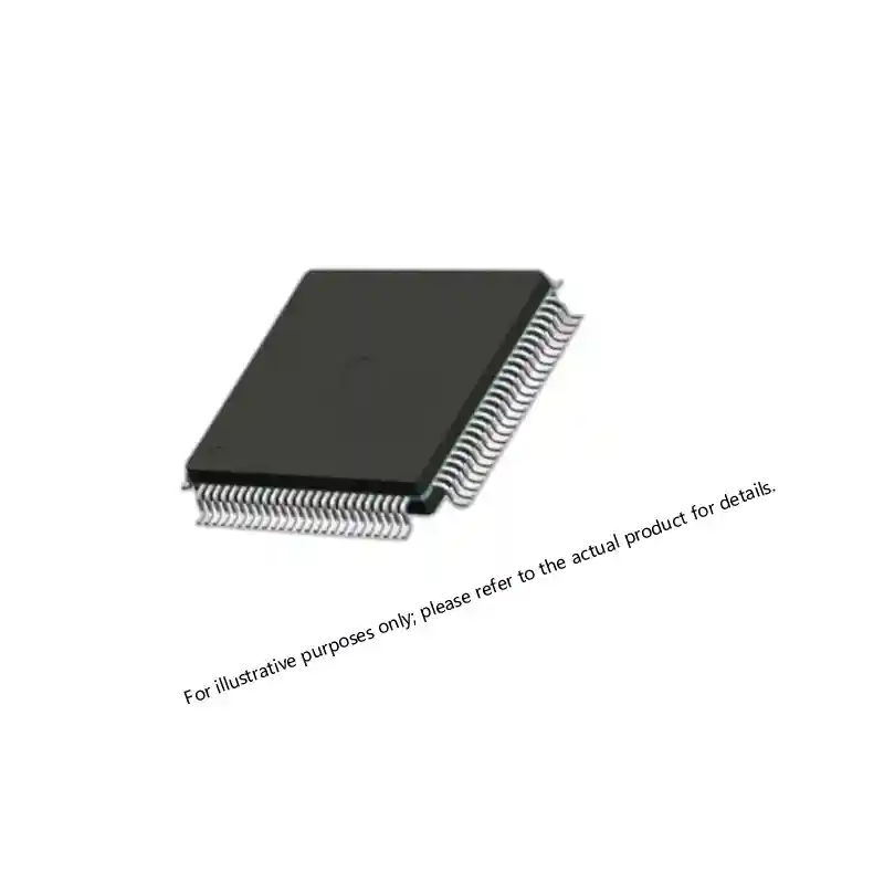
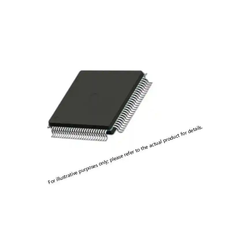
The W3H64M72E-400BI is a 64M×72 DDR2 SDRAM in a supplier-specific package and grade code, and the part number settles less than most buyers assume. It establishes the memory family, the word count, the 72-bit bus width, and a 400 speed bin. It does not establish the operating temperature range, the screening level, the package finish, or the lot documentation a program reviewer will request later. Those details live in the datasheet revision and in the conformance records, not in the ordering string. This guide separates what the designation proves from what the program still has to verify, so a sourcing decision rests on documents rather than on a familiar part number.
What the W3H64M72E-400BI Designation States
A defense BOM line compresses a specification into a string, and the string is only as good as the document behind it. Read the W3H64M72E-400BI from left to right and three facts are settled: the device belongs to the W3 high-reliability memory series, it is a DDR2 SDRAM, and it is organized as 64M words on a 72-bit bus at a 400 speed bin.
The width deserves attention because it drives the board. Seventy-two lanes let a controller move 64 data bits and 8 check bits inside the same burst, so error correction costs no additional transfer. That is a decision made at layout, long before anyone issues a purchase order, and it explains why 72-bit DDR2 parts remain in programs that could otherwise move to a narrower, faster interface.
| Element | What it states | What it does not establish |
|---|---|---|
| W3 series | Supplier high-reliability memory family | Screening level or qualification status |
| DDR2 SDRAM | JEDEC DDR2 interface family | Which JEDEC revision the die was characterized against |
| 64M × 72 | 64M addressable words on a 72-bit bus | Usable capacity after controller mapping and ECC handling |
| 400 | 400 MT/s data rate bin | Sustained throughput on your board |
| BI suffix | Supplier package and grade code | Temperature range, lead finish, or hermeticity before the ordering code is read |
The suffix is where catalog reading goes wrong. Letters such as BI encode package and grade inside one supplier’s ordering scheme, and similar letters can mean something different in another scheme or another revision. Treat the suffix as a pointer to the ordering code page, never as a statement about temperature range or screening.
Why a 72-Bit DDR2 Bus Still Fits Defense Architectures
Error correction is the first argument. With 8 check bits beside every 64 data bits, the controller corrects a single-bit error and detects a double-bit error within the same read. Where bit flips are a design consideration rather than a theoretical one, that protection sits in the data path continuously instead of being scheduled as a separate task.
Correction alone is not sufficient. A corrected error still leaves a repaired location behind, so the controller or a background routine has to scrub the array to stop single-bit errors from accumulating into an uncorrectable pair. Scrubbing policy is a system decision, and the memory device cannot make it on the program’s behalf.
The second argument is architectural simplicity. A 72-bit bus concentrates storage into fewer packages than a set of narrow components, which cuts solder joints, cuts the number of lot records the receiving team must reconcile, and cuts the number of lines that can reach end of life on different dates.
The cost is real. Seventy-two lanes consume routing layers, need termination and skew control, and lengthen the layout review. When the program controls the board and can select a newer interface, narrower lanes at a higher rate may deliver comparable throughput on less copper. When the controller is fixed by an existing design or a legacy backplane, the wide bus is usually the cheaper route because it avoids requalification of the processing chain.
Boards that carry this memory generally carry a logic device beside it, and the two age on different schedules even when they were released together. <XCKU115 UltraScale FPGA: Powering Critical Defense Systems> covers how that class of device is used in defense systems.
Peak Bandwidth Arithmetic and What Limits It in Practice
The theoretical figure follows from the designation itself. At 400 million transfers per second across 72 bits, the bus moves 28.8 Gbit/s, which is 3.6 GB/s after dividing by eight. If 8 of those lanes carry check bits, payload bandwidth is 3.2 GB/s and the remaining 0.4 GB/s is the cost of protection. Both numbers are ceilings, and both assume the controller clocks every lane at the stated rate.
Several mechanisms remove time from that ceiling. Refresh cycles occupy the bus on a fixed schedule. Bank conflicts stall a request when two accesses in flight target the same bank. Read to write turnaround costs idle cycles that no amount of controller tuning removes entirely. Arbitration with other bus masters, the latency of the ECC logic itself, and the efficiency of the memory controller’s scheduler all take a share. A program that plans its processing budget against the 3.6 GB/s figure will plan against a number the hardware never delivers.
The practical approach is to measure on the target board. Run a bandwidth test that mirrors the real access pattern, capture a bus trace during the heaviest task the program performs, and record the test conditions beside the result: clock configuration, refresh setting, controller mode, and the surrounding traffic. Those records turn a performance claim into a design margin, and they are the same records a reviewer asks for when a processing budget is challenged after a board respin.
Reading the Datasheet Before You Approve the Part
Initialization and Mode Register Settings
DDR2 devices arrive in an undefined state and must be initialized in a fixed order. The controller applies power in sequence, waits for the internal delay locked loop to settle, then writes the mode register and extended mode registers with the burst length, CAS latency, and output drive settings the board was routed for. On-die termination and off-chip driver calibration settings belong in the same sequence. A program that copies an initialization routine from a different memory density or a different controller risks a mode register value that the device accepts but the board cannot support at rate. Confirm the sequence against the datasheet revision that applies to the lot, not against a routine inherited from an earlier build.
Timing Budget at the Board Level
The datasheet timing table gives limits at the package pins. Your budget has to add flight time, connector loss, and skew across 72 lanes, then compare the result with the controller’s timing window rather than with the device’s own limits. Temperature derating matters here as well, because a timing table that holds at one end of the range may require a slower setting at the other. Where the margin is thin, the honest option is to reduce the operating clock, document the reduction, and carry it into the qualification plan rather than to accept a design that only passes on the bench.
What the Datasheet Leaves to the System
Several behaviors belong to the system and never appear as a device limit. Refresh rate against case temperature is one, because a hotter part needs more frequent refresh and the controller sets the interval. Scrubbing frequency is another, since it depends on the error rate the program is willing to tolerate. ECC policy, address mapping, and the handling of a detected double-bit error are all system decisions. Reading the datasheet carefully means recognizing the boundary: the document defines what the device guarantees, and the program defines what it needs beyond that.
Separating Identity from Conformance in Lot Records
Memory procurement fails most often at the seam between two questions that look identical. The first is whether this is the right part. The second is whether this lot meets the requirement. A photograph, a label, and a familiar suffix answer the first. They say nothing about the second, and treating them as equivalent is how a compliant part number ends up attached to a noncompliant lot.
The work moves through three stages. Identity asks whether the item in hand matches the ordered part number and revision. Conformance asks whether the lot meets the specified screening, test, and documentation requirements. Release asks whether the program’s own authority accepts the evidence and permits the part onto the build. Each stage has different evidence, different cost, and a different owner.
| Record | Method context | Responsible use | Do not infer |
|---|---|---|---|
| Stock label and photograph | Label, date code, and package marking as received | Confirms the item matches the ordered part number at the identity stage | That the die is authentic or that any screening was performed |
| Manufacturer datasheet revision | Published electrical and mechanical limits | Defines the limits your inspection and test plan compares against | That a specific lot was tested to those limits |
| Certificate of conformance | Supplier declaration against a named specification | Records what the supplier warrants for the lot | Independent verification of the underlying measurements |
| Incoming inspection result | Your own measurement, method, and sampling plan | Establishes what your laboratory observed on the sampled units | Lot-wide conformance beyond the sampling plan |
| Board-level functional test | Your system, firmware, and environmental profile | Establishes behavior in your application at your conditions | That another board build or another program will behave the same |
Two consequences follow. A worn, re-marked, or long-stored item can help you identify a part, but its measurements are not automatically a valid acceptance standard, because storage history and handling affect what those measurements mean. Equally, an older date code can pass all three stages when the records are complete and the program accepts the age. Age is a fact to be recorded, not a verdict to be assumed.
Building an RFQ That Produces Comparable Quotes
Quotes arrive incomparable when the request leaves screening and documentation open. Two suppliers can price the same part number at very different figures simply because one is quoting a tested lot with papers and the other is quoting a declared lot with none. Specify the differences before the comparison starts.
| RFQ field | What to request | Why it matters |
|---|---|---|
| Part number and revision | Full ordering code plus the datasheet revision in force | Two revisions can carry different limits under the same title |
| Screening level | The exact test specification and level the program requires | Separates a tested lot from a declared lot before price is discussed |
| Temperature range | Required operating range and the derating basis | Sets which grade is eligible at all |
| Documentation set | Conformance certificate, lot traceability, and test data | Makes the offer auditable at the release stage |
| Package and finish | Package type, lead finish, and any hermeticity requirement | Affects solderability, storage life, and rework rules |
| Date code window | Acceptable date code range or maximum lot age | Prevents a compliant part from arriving outside program limits |
A short contrast makes the gap visible. Reject this line: “W3H64M72E-400BI, quantity 50, best price, commercial equivalent acceptable if delivery is faster.” Replace it with: “W3H64M72E-400BI at the ordering code and datasheet revision named in the program baseline, quantity 50, screened to the specified test level, operating range per baseline, certificate of conformance and lot traceability included, package finish per drawing, date code within the program window, with lead time and any minimum quantity stated in the offer.” The second version takes five minutes longer to write and removes most of the follow-up correspondence.
Planning Supply Through a DDR2 Obsolescence Window
DDR2 sits on the mature side of the memory roadmap, and mature interfaces eventually lose their production allocation. The signal is rarely dramatic. A product change notice arrives, then a distributor’s stock thins, then a broker offers the same part number at a figure that no authorized channel matches. Programs that have already documented their options treat this as a planning event. Programs that have not treat it as an emergency.
Three responses are available and they carry different costs. A last-time buy secures the quantity, ties up capital, and creates a storage obligation that includes humidity control, ESD handling, and periodic inspection of packaging integrity. Die or wafer banking defers packaging and test to a later date, which preserves the silicon but pushes risk into the future qualification of a newly packaged lot. A redesign to a newer interface removes the dependency permanently and costs a board spin, a firmware change, and a full requalification cycle. None of the three is universally correct. A short remaining production run favors the last-time buy. A program with a decade of sustainment ahead usually favors the redesign, with a bridge buy covering the transition.
The executable checks are straightforward. Request the manufacturer’s lifecycle status and the product change notice history for the exact ordering code. Confirm the storage conditions your facility can actually maintain, not the ones in a procedure. Compare the projected consumption rate against the program schedule before committing to a bridge quantity, because an oversized buy becomes an excess inventory problem with the same paperwork burden as a shortage. Availability planning also works better when every long-lead line has a documented second option rather than a verbal one. <XC7VX485T Virtex-7 FPGA: Performance and Sourcing for Defense> covers performance and sourcing considerations for that family.
Consolidation helps at the record level as much as the price level. When memory, logic, converters, and power modules for one build arrive through a single traceable channel, the receiving team reconciles one set of lot records instead of five, and a missing certificate is caught before the build rather than after. Sparkle Electronics stocks memory alongside FPGA, DSP, converter, and power families for exactly that reason, which matters most when a line is waiting on one part rather than on the whole BOM. <A1020B-PG84B ACT2 FPGA: Specs, Sourcing, and Availability> covers the specification, sourcing, and availability picture for a comparable legacy device.
Request a Documented Quote for Your Memory Requirements
Send the full ordering code with the datasheet revision, the quantity and delivery schedule, the screening level and test specification the program requires, the operating temperature range, the package and lead finish requirement, the acceptable date code window, and the documentation set that must accompany the lot. Those fields are what make two offers comparable, and they are the same fields the release authority will ask about months later. If the program is still weighing a last-time buy against a redesign, say so and include the schedule you are protecting, because the answer changes the quantity that makes sense.
A quote is not an approval and a stocked part is not a released part. The reply will name the revision, the screening basis, and the traceability documents attached to the offer so the decision can be made on evidence.
David Lin, Sparkle Electronics, xuansc2144@gmail.com
FAQ
Is the W3H64M72E-400BI a military-grade component?
The designation alone does not answer that question. It tells you the family, the 64M×72 organization, the 72-bit bus, and the speed bin. Military-grade status depends on the screening level, the qualified temperature range, and the conformance documentation attached to the specific lot. Ask for the datasheet revision, the ordering code page, and a certificate of conformance that names the test specification. Where the answer feeds a program baseline, treat a catalog description as a starting point and the lot records as the evidence.
What does the 400 in the part number refer to?
It identifies the speed bin, and in this family the bin is expressed as a data rate in transfers per second rather than as a clock frequency. The datasheet timing table converts that bin into the parameters a controller needs, including clock period, CAS latency options, and strobe timing. Two devices in the same bin can still differ in package, grade, and screening, so confirm the full ordering code rather than the headline number. If the controller runs at a fixed clock, check the bin against the controller’s supported range before requesting quotes.
Can a commercial DDR2 device replace it?
Only if the program’s approval basis permits the substitution. A commercial device may share the footprint and the interface while differing in operating range, screening, package finish, and lot documentation. Upscreening can close part of that gap and cannot recreate the manufacturer’s qualification history. The usual sequence is a documented equivalence review, a board-level qualification run using the program’s environmental profile, and formal approval by the authority that controls the baseline. Footprint compatibility is a layout fact, not a qualification argument.
What documentation should arrive with the shipment?
At minimum, a certificate of conformance that names the specification, lot and date code traceability, the applicable datasheet revision, and packaging records covering ESD and moisture handling. Where the program specifies screening, the test data or a summary of it should travel with the lot. Keep your own incoming inspection record beside those documents, because the release decision belongs to your program and rests on a chain of records rather than on a supplier declaration taken alone.
If you’re interested, check out these related articles:
Virtex-7 XC7VX690T: Performance and Reliability Insights
XC7VX485T FPGA: Virtex-7 Performance for Defense
XCKU115 UltraScale FPGA: Powering Critical Defense Systems
Virtex-7 XC7VX690T: Performance, Reliability, and Integration
XCKU085 UltraScale FPGA: Performance for Critical Systems